

Semiconductor device, print head and image forming apparatus
- Summary
- Abstract
- Description
- Claims
- Application Information
AI Technical Summary
Benefits of technology
Problems solved by technology
Method used
Image


Examples
embodiment 1
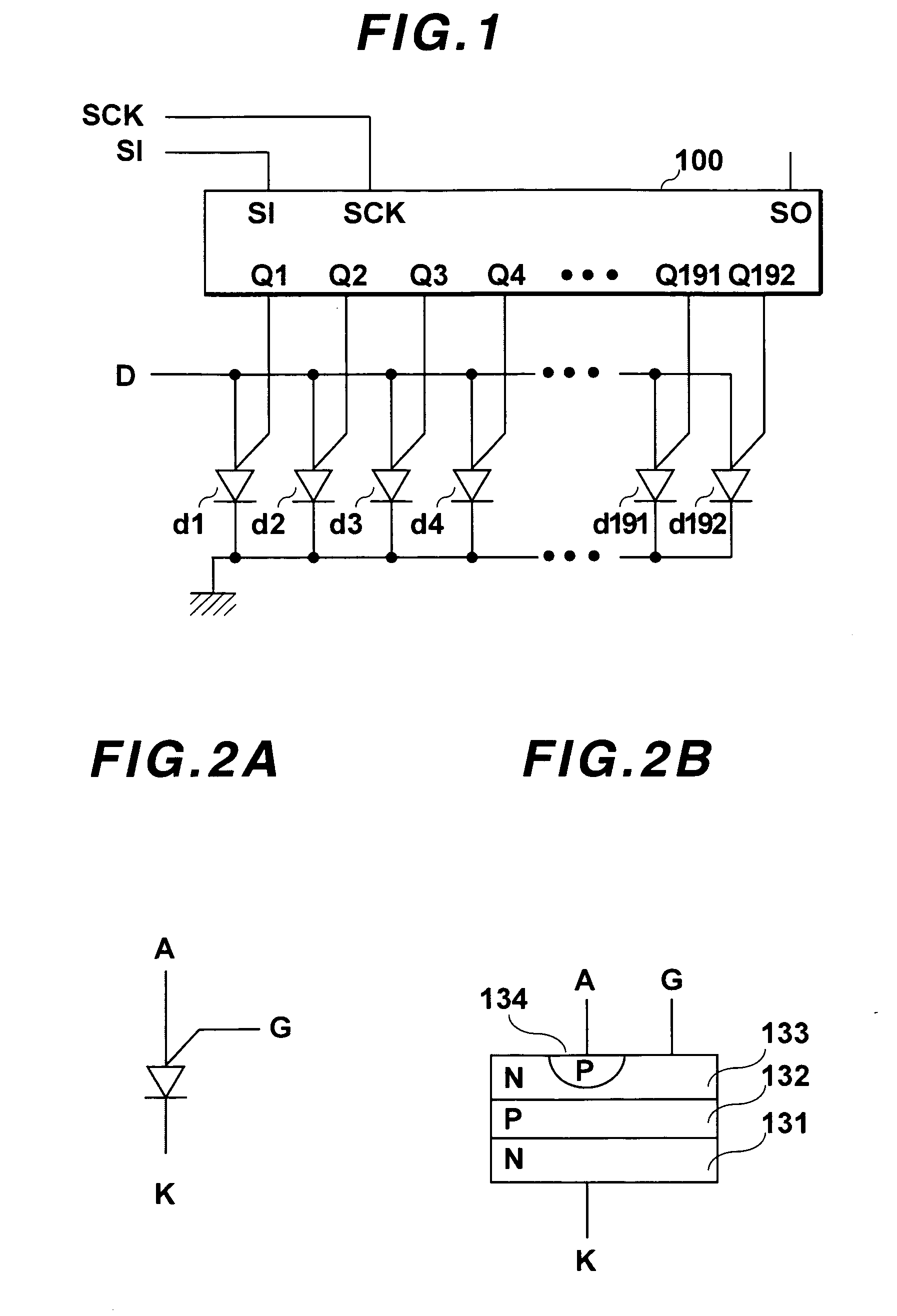
[0043]FIG. 1 is a circuit diagram showing a structure of semiconductor device to construct a print head in embodiment 1 of the present invention.
[0044]As shown by the FIG. 1, a semiconductor device to construct a print head in embodiment 1 has a shift register circuit 100 and 192 pieces of luminous thyristors of luminous thyristors d1, d2, . . . , d192 serving as light emitting element. In the shift register circuit 100, 192 pieces of flip-flop circuits FF to construct conventional LED head shown by FIG. 13 are connected in series. The respective flip-flop circuits FF includes data output terminals Q1, Q2, . . . , Q192 furnished in the shift register circuit 100 and mentioned below, and keeps a voltage level for supplying voltage to make the luminous thyristors d1, d2, . . . , d192 emit light. Further, the output terminal Qn of the flip-flop circuits FF is outputted by shifting and inputting signal of output terminal Qn-1 serving as a fore segment.
[0045]Further, the shift register c...
embodiment 2
[0068]FIG. 5 is a circuit diagram showing a structure of print head in embodiment 2 of the present invention.
[0069]As shown by the FIG. 5, a semiconductor device to construct a print head 20 in embodiment 2 has a shift register circuit 200 and 192 pieces of luminous thyristors of luminous thyristors d1, d2, . . . , d192 serving as light emitting element. In the shift register circuit200, data output terminals Q1, Q2, . . . , Q96 are furnished. The data output terminals Q1, Q2, . . . , Q96 are respectively connected with gate terminal G of adjoining two luminous thyristors. For example, the data output terminal Q1 is connected with the gate terminal G of the luminous thyristors d1 and d2, the data output terminal Q2 is connected with the gate terminal G of the luminous thyristors d3 and d4. Further, in the shift register circuit 200, 96 pieces of the flip-flop circuits FF of the embodiment 1 are connected in series.
[0070]The luminous thyristors d1, d2, . . . , d192 are the same as th...
example of embodiment 2
Transformation Example of Embodiment 2
[0085]FIG. 7 is a circuit diagram showing a structure of a transformation example of print head in embodiment 2 of the present invention.
[0086]As shown by the FIG. 7, a semiconductor device to construct a print head 30 in a transformation example of embodiment 2 has a shift register circuit 300 and 192 pieces of luminous thyristors of luminous thyristors d1, d2, . . . , d192 serving as light emitting element. In the shift register circuit 300, data output terminals Q1, Q2, . . . , Q48 are furnished. The data output terminals Q1, Q2, . . . , Q48 are respectively connected with gate terminal G of adjoining four luminous thyristors. For example, the data output terminal Q1 is connected with the gate terminal G of the luminous thyristors d1, d2, d3 and d4, the data output terminal Q2 is connected with the gate terminal G of the luminous thyristors d5, d6, d7 and d8. Further, in the shift register circuit 300, 48 pieces of the flip-flop circuits FF o...
PUM
 Abstract
Description
Claims
Application Information