Coa array substrate and method of fabricating same

Inactive Publication Date: 2021-11-18
SHENZHEN CHINA STAR OPTOELECTRONICS SEMICON DISPLAY TECH CO LTD
View PDF0 Cites 0 Cited by
  • Summary
  • Abstract
  • Description
  • Claims
  • Application Information

AI Technical Summary

Benefits of technology

The present invention provides a COA array substrate and a method for manufacturing the same by filling a spacing layer in a through hole to avoid the problems of twill traces and rising product cost. This avoids the need for expensive equipment and materials, which saves time and money. Overall, this technology improves the manufacturing process for COA array substrates.

Problems solved by technology
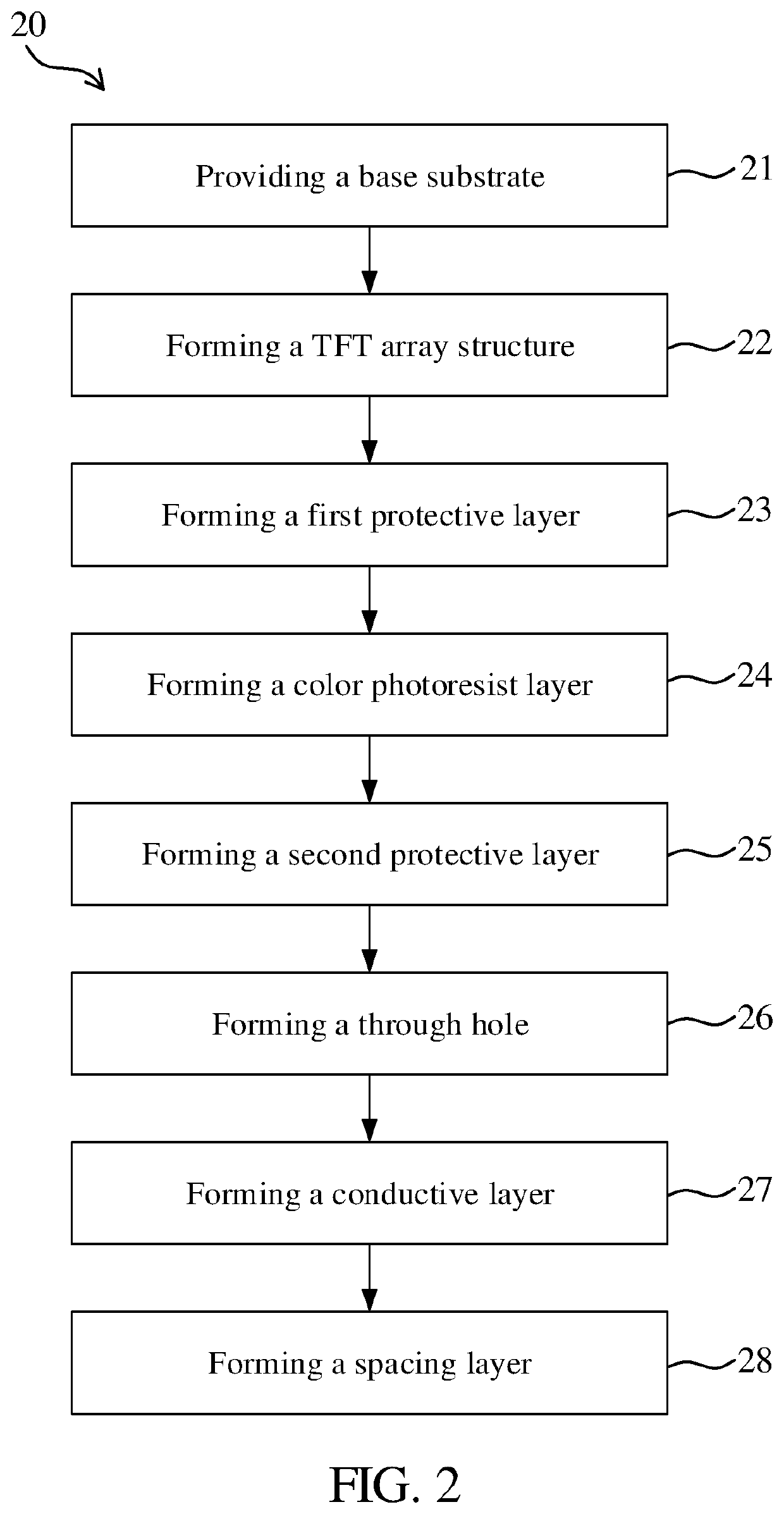
However, this design also leads to an increase in depth of via holes of the substrate, which easily cause problems in subsequent coating of the polyimide (PI) thin film, resulting in uneven light in the display panel, so as to produce twill traces (also known as mura).
In addition, as depth of the through hole increases, more liquid crystal molecules need to be filled into the through hole so as to achieve a same effect, so the product cost increases.

Method used


Image

  • Coa array substrate and method of fabricating same
  • Coa array substrate and method of fabricating same

Examples


Embodiment Construction

[0024]Following description of the various embodiments is provided to illustrate the specific embodiments of the present disclosure. Furthermore, directional terms mentioned in the present disclosure, such as upper, lower, top, bottom, front, rear, left, right, inner, outer, side, surrounding, central, horizontal, horizontal, vertical, longitudinal, axial, radial, an uppermost layer or a lowermost layer, etc., only refer to a direction of the accompanying figures. Therefore, the used directional terms are used to describe and understand the present disclosure, but the present disclosure is not limited thereto.

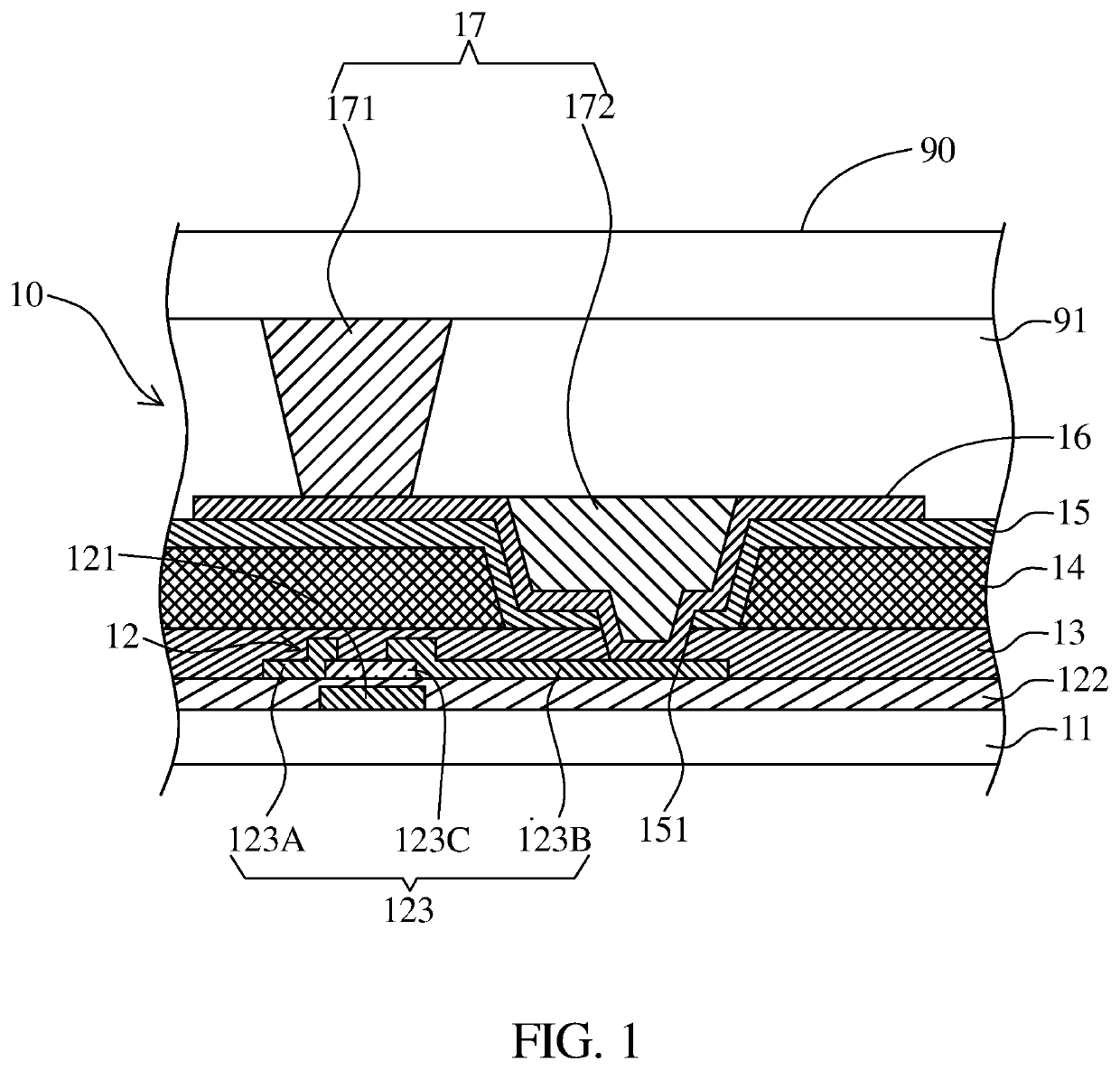
[0025]Referring to FIG. 1, an embodiment of the present disclosure provides a color-filter-on-array (COA) array substrate 10 comprising a base substrate 11, a thin film transistor (TFT) array structure 12, a first protective layer 13, a color photoresist layer 14, a second protective layer 15, a conductive layer 16, and a spacing layer 17. In an embodiment, the base substrate 1...


PUM


Abstract

A color-filter-on-array (COA) array substrate and a method of fabricating the same are provided. The COA array substrate has: a base substrate; a thin film transistor (TFT) array structure disposed on the base substrate; a first protective layer disposed on the TFT array structure; a color photoresist layer disposed on the first protective layer; a second protective layer disposed on the color photoresist layer, wherein a through hole pass through the second protective layer, the color photoresist layer, and the first protective layer; a conductive layer disposed on the second protective layer and in the through hole, wherein the conductive layer is electrically connected to the TFT array structure; and a spacing layer disposed on the conductive layer and filled in the through hole. The COA array substrate can avoid problems of twill traces and rising product costs.

Description

FIELD OF DISCLOSURE[0001]The present disclosure relates to an array substrate and a method of fabricating the same, and more particularly to a color-filter-on-array (COA) array substrate and a method of fabricating the sameBACKGROUND OF DISCLOSURE[0002]A liquid crystal panel includes an array substrate, a color filter substrate, and a liquid crystal layer sandwiched between the array substrate and the color filter substrate. Among them, an electric field is generated by a circuit to drive liquid crystal molecules, so that the liquid crystal has different optical effects.[0003]A color-filter-on-array (COA) technology is a technology for fabricating a color filter on a side of a thin film transistor (TFT) to reduce parasitic capacitance and increase product aperture ratio. In addition, many companies have combined a use of COA and a polymer-film-on-array (PFA) technology to further improve the aperture ratio. However, this design also leads to an increase in depth of via holes of the ...

Claims


Application Information

Patent Timeline
IPC IPC(8): G02F1/1362G02F1/1368H01L27/12
CPCG02F1/136227G02F1/136222H01L27/1259H01L27/124H01L27/1248G02F1/1368G02F1/1362
Inventor LI, LANYAN
Owner SHENZHEN CHINA STAR OPTOELECTRONICS SEMICON DISPLAY TECH CO LTD
Why Eureka
Try Eureka