

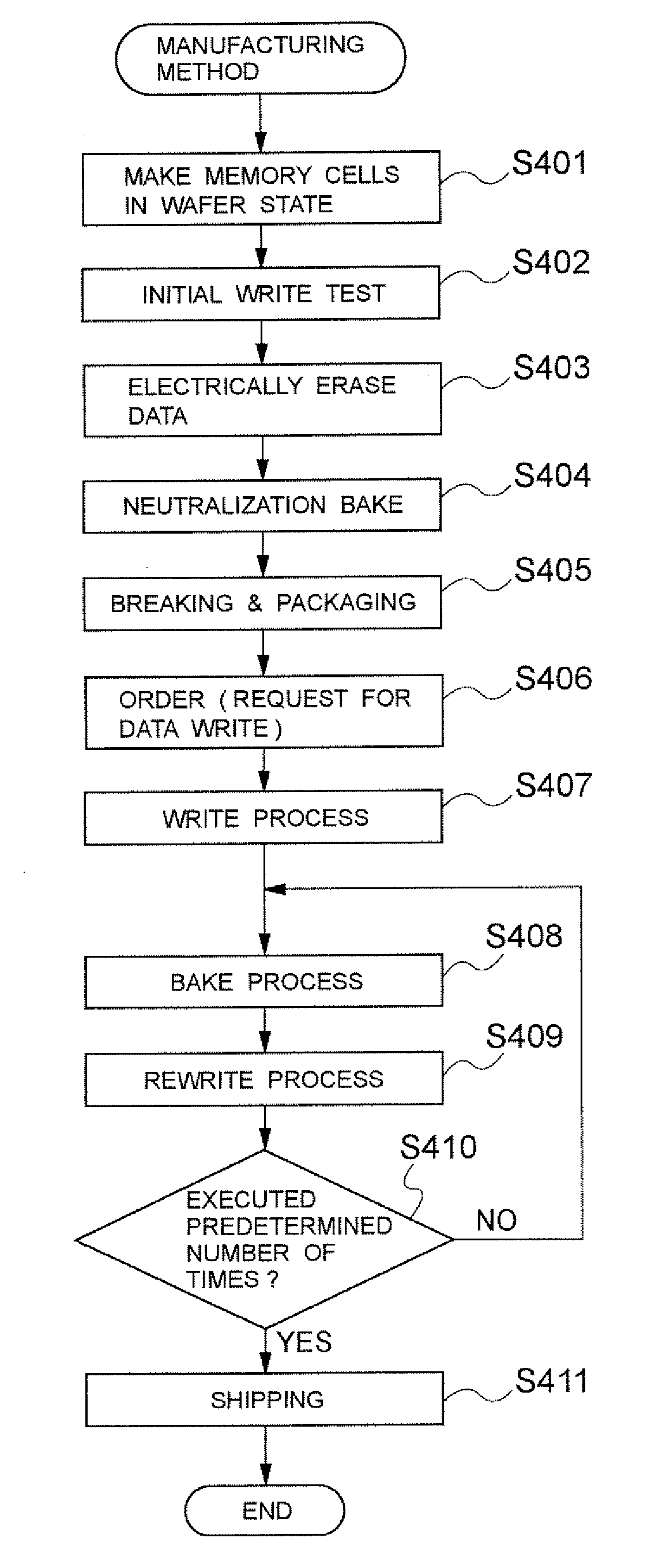
Manufacturing method, remanufacturing method and reshipping method for a semiconductor memory device
a manufacturing method and memory device technology, applied in semiconductor devices, digital storage, instruments, etc., can solve the problems of easy disturbance of information data writing, and achieve the effect of preventing program falsification
- Summary
- Abstract
- Description
- Claims
- Application Information
AI Technical Summary
Benefits of technology
Problems solved by technology
Method used
Image

Examples
Embodiment Construction
[0019]With reference to the drawings, explanation will now be made in detail on an embodiment according to the present invention.
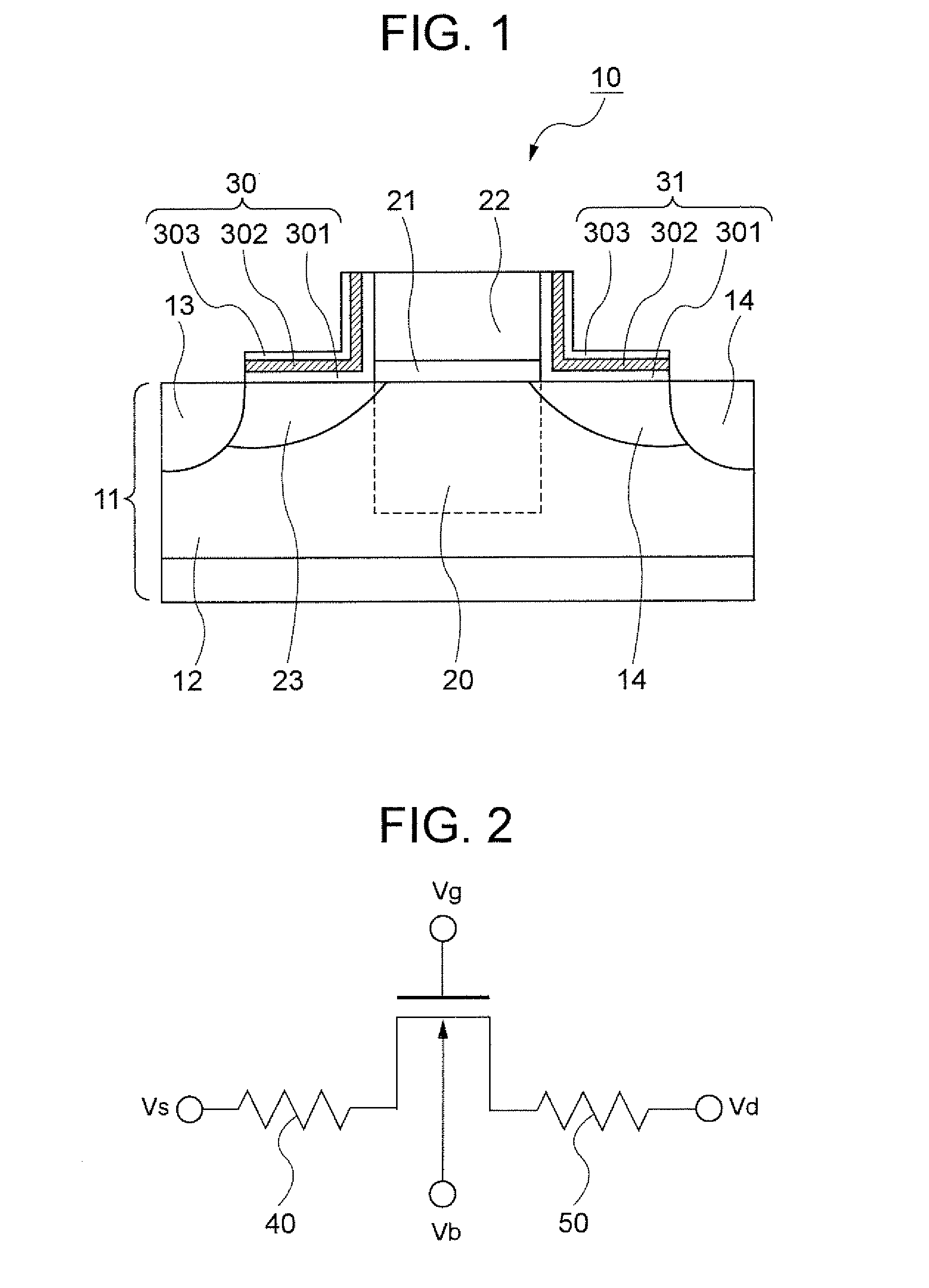
[0020]FIG. 1 shows a structure of a memory cell 10 making up a semiconductor memory device to be manufactured by a manufacturing method for a semiconductor memory device according to the invention. The memory cell 10 is of an FET structure having a gate electrode 22 formed on a semiconductor substrate 11, first and second charge storage parts 30, 31 formed on the both sides of the gate electrode 22, a source electrode region 13, a drain electrode region 14, a first resistance-change region 23 and a second resistance-change region 24.
[0021]A p-well region 12 is formed in a surface of a semiconductor substrate 11, e.g. p-type silicon substrate. In the surface of the p-well region 12, the source and drain electrode regions 13, 14 are provided containing a high concentration of an n-type impurity (n+ type). The source electrode region 13 and the drain electrod...
PUM
 Abstract
Description
Claims
Application Information