Method for realizing a contact of an integrated well in a semiconductor substrate, in particular for a base terminal of a bipolar transistor, with enhancement of the transistor performances

a well and integrated technology, applied in the direction of transistors, electrical devices, semiconductor/solid-state device manufacturing, etc., can solve problems such as worsening performance, and achieve the effect of reducing parasitic current and reducing extension

Active Publication Date: 2008-10-09
STMICROELECTRONICS SRL
View PDF1 Cites 0 Cited by
  • Summary
  • Abstract
  • Description
  • Claims
  • Application Information

AI Technical Summary

Benefits of technology

[0032]One embodiment realizes a contact of a well of a first type of dopant integrated in a semiconductor substrate next to a further well of a second type of dopant and forming with it a parasitic diode, such contact being suitably shaped so as to reduce its extension with respect to the length of the well, thus reducing the parasitic current of the parasitic diode, in particular in the case of the P-well / N-well junction which is created between the base contact well and the emitter contact well of a bipolar transistor, for example comprised in a power actuator.

Problems solved by technology

It is to be noted that this power actuator 1 however contains different parasitic components which worsen the performances.

Method used


Image

  • Method for realizing a contact of an integrated well in a semiconductor substrate, in particular for a base terminal of a bipolar transistor, with enhancement of the transistor performances
  • Method for realizing a contact of an integrated well in a semiconductor substrate, in particular for a base terminal of a bipolar transistor, with enhancement of the transistor performances
  • Method for realizing a contact of an integrated well in a semiconductor substrate, in particular for a base terminal of a bipolar transistor, with enhancement of the transistor performances

Examples


Embodiment Construction

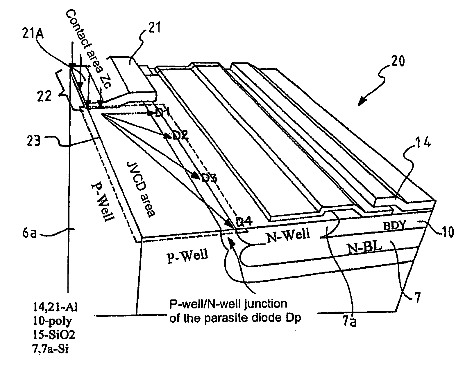
[0050]With reference to these figures, and in particular to FIGS. 5A and 5B, 20 globally and schematically indicates a power actuator realized according to one embodiment, in particular a portion thereof in correspondence with a base contact terminal B of the bipolar transistor comprised therein.

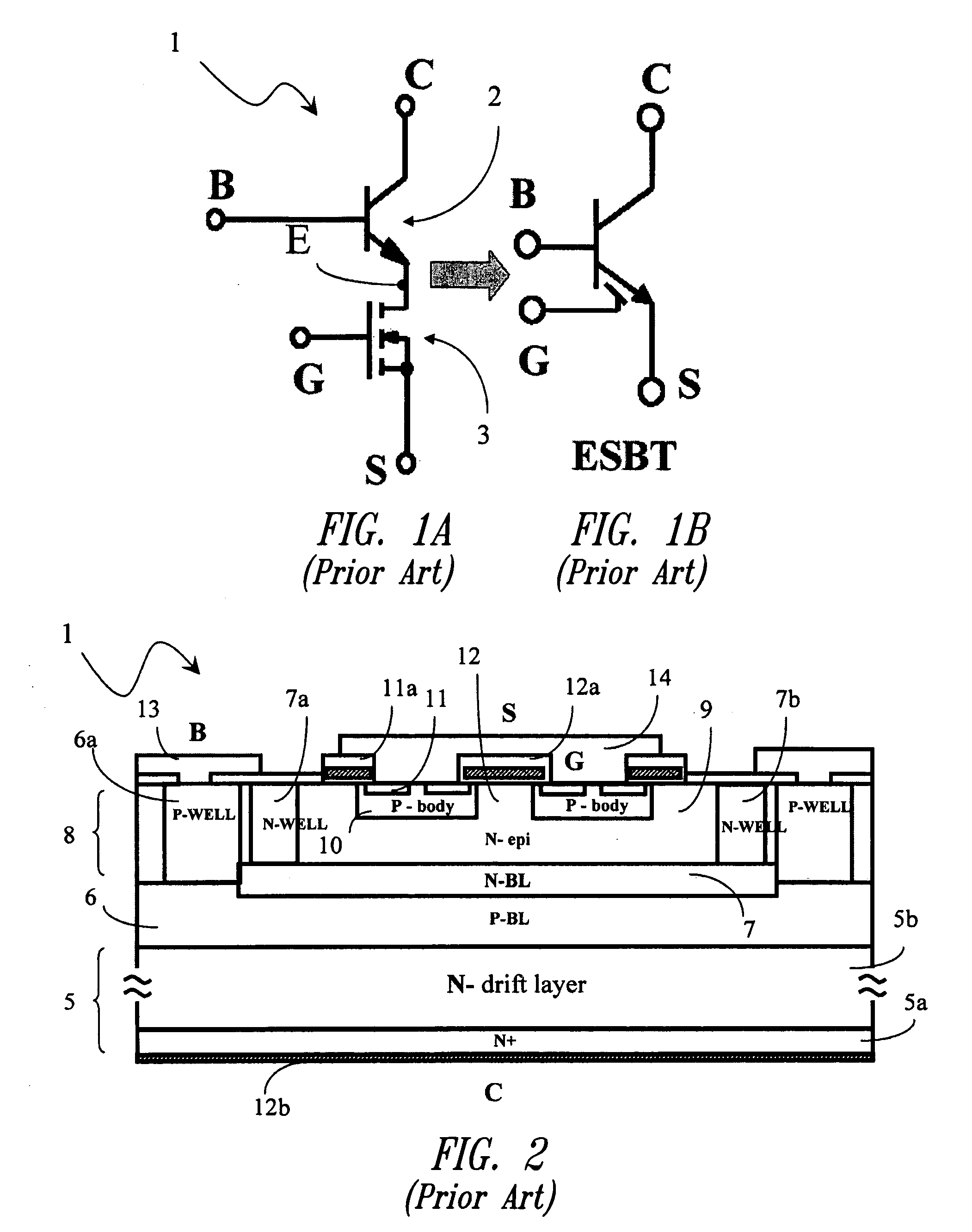
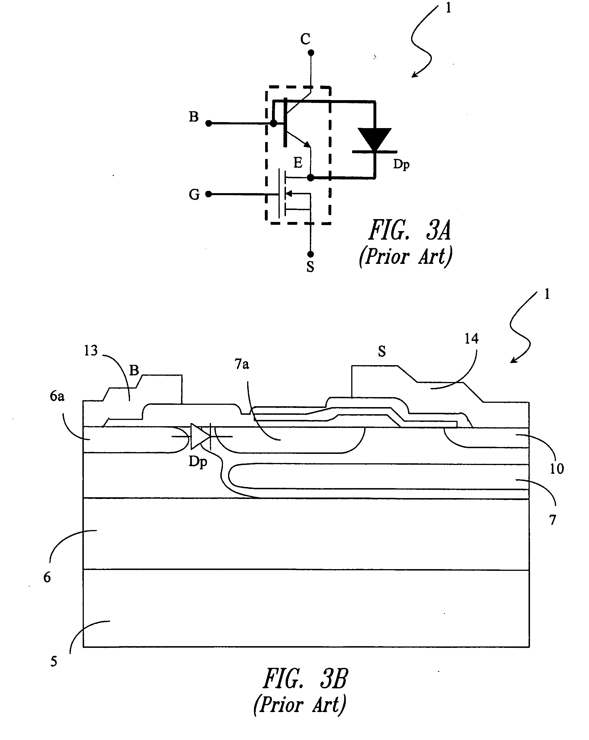
[0051]By way of illustration, elements being structurally and functionally identical with respect to the power actuator described with reference to the prior art will be given the same reference numbers.

[0052]Moreover, the figures showing schematic views of portions of an integrated structure are not drawn to scale, but are instead drawn so as to highlight important features.

[0053]It is suitable to underline that the considerations reported hereafter can be applied, in the same way, to a generic contact of a well of a first type of dopant integrated in a semiconductor substrate next to a further well of a second type of dopant and forming with it a parasitic diode and one embodiment proposes...


PUM


Abstract

A method realizes a contact of a first well of a first type of dopant integrated in a semiconductor substrate next to a second well of a second type of dopant and forming with it a parasitic diode. The method comprises: formation of the first well; formation of the second well next to the first well; definition of an oxide layer above the first and second wells; and formation of an electric contact layer above the oxide layer in correspondence with the first well for realizing an electric contact with it. The definition step of the oxide layer further comprises a deposition step of this oxide layer above the whole first well and a removal step of at least one portion of the oxide layer in correspondence with a contact area of the first well so that the contact area has a shorter length than a length of the first well.

Description

BACKGROUND[0001]1. Technical Field[0002]The present invention relates to a method for realizing a contact of a well, integrated in a semiconductor substrate, in particular for a base terminal of a bipolar transistor.[0003]More specifically, the invention relates to a method for realizing a contact of a first well of a first type of dopant, integrated in a semiconductor substrate, next to a second well of a second type of dopant and forming with it a parasite diode.[0004]The invention also relates to bipolar transistor and to a power actuator of the emitter-switched type comprising at least one high voltage bipolar transistor.[0005]2. Description of the Related Art[0006]As it is well known, a power actuator of the emitter-switched type is an electronic device able to supply a low voltage drop in conduction together with a high operative frequency.[0007]In particular, as schematically shown in FIG. 1A, a power actuator of the emitter-switched type, globally indicated with 1, essential...

Claims


Application Information

Patent Timeline
Patent Type & Authority Applications(United States)
IPC IPC(8): H01L29/73H01L21/22
CPCH01L21/8249H01L27/0716H01L29/42304H01L29/732
Inventor ENEA, VINCENZORONSISVALLE, CESARE
Owner STMICROELECTRONICS SRL
Why Eureka
Try Eureka