Semiconductor device and method of producing a semiconductor device

a semiconductor and semiconductor technology, applied in semiconductor devices, semiconductor/solid-state device details, electrical equipment, etc., can solve the problems of unintended injection into the nitride layer of state-of-the-art nrom cells above the channel region, inability to program rom electrically, and expensive and time-consuming redesign of special masks

Inactive Publication Date: 2006-05-04
QIMONDA
View PDF14 Cites 10 Cited by
  • Summary
  • Abstract
  • Description
  • Claims
  • Application Information

AI Technical Summary

Benefits of technology

[0033] The inventive memory cell and the respective memory cell array provide for a good alignment of charge carriers in

Problems solved by technology

The ROM cannot be programmed electrically.
Changes in data programming result in the expensive and time-consuming redesign of the special masks.
An unintended injection into the nitride layer of state-of-the-art NROM cells above the channel region cannot be avoide

Method used


Image

  • Semiconductor device and method of producing a semiconductor device
  • Semiconductor device and method of producing a semiconductor device
  • Semiconductor device and method of producing a semiconductor device

Examples


Embodiment Construction

[0053] Preferred embodiments are discussed in detail below. It should be noted, though, that the present invention provides many applicable concepts that can be embodied in a wide variety of specific contexts. The specific embodiments discussed are merely illustrative of specific ways to make and use the invention and do not limit the scope of the invention.

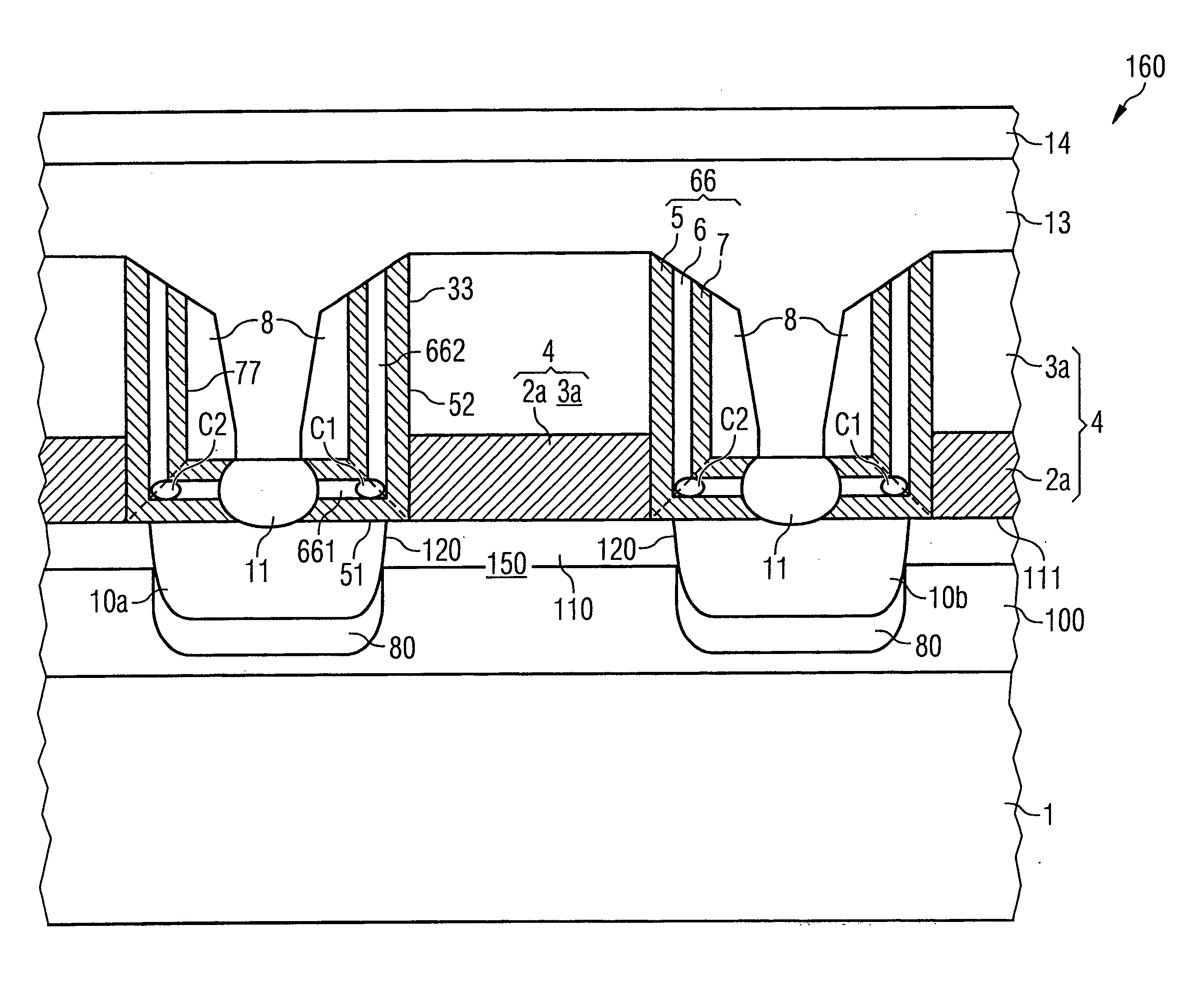
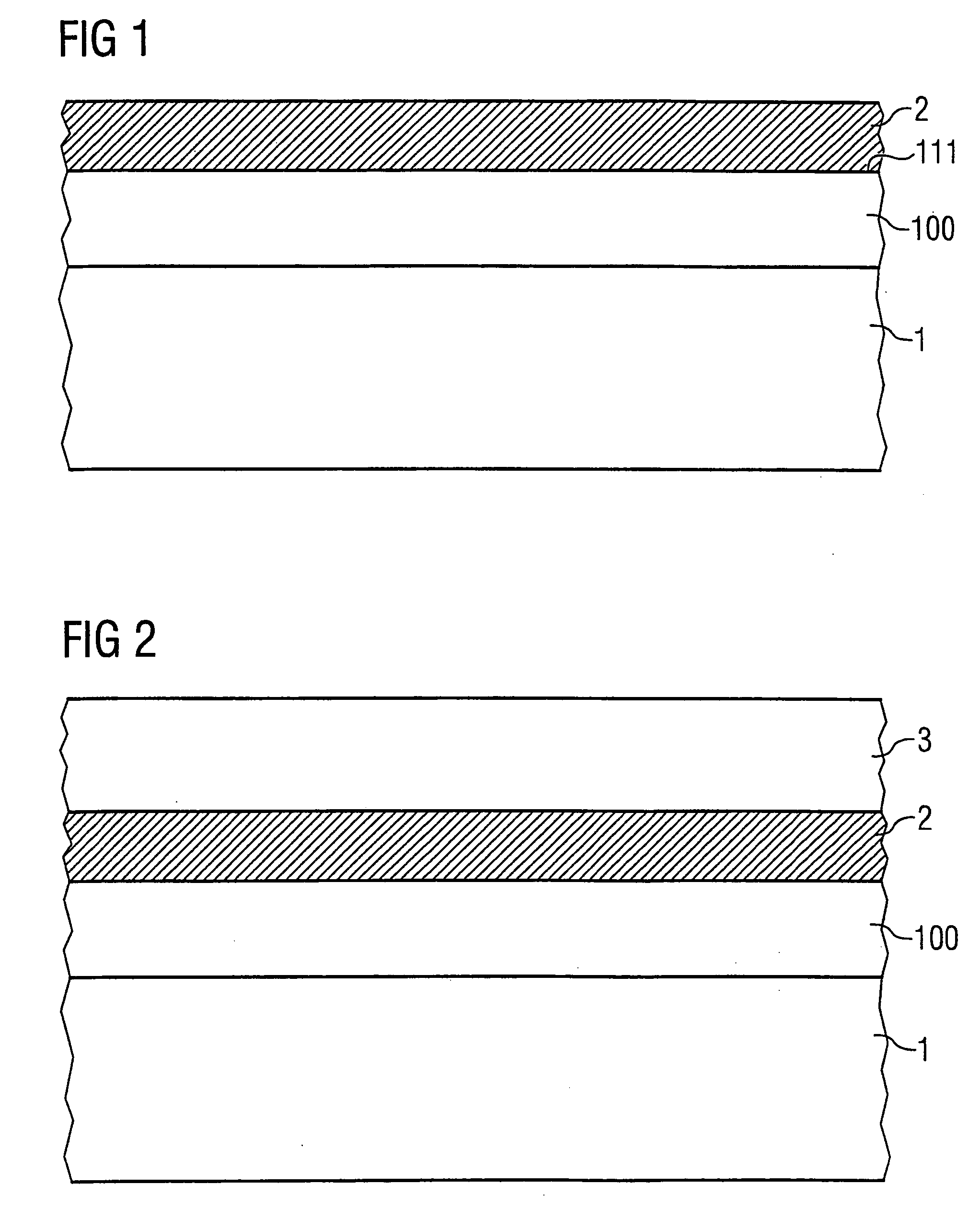
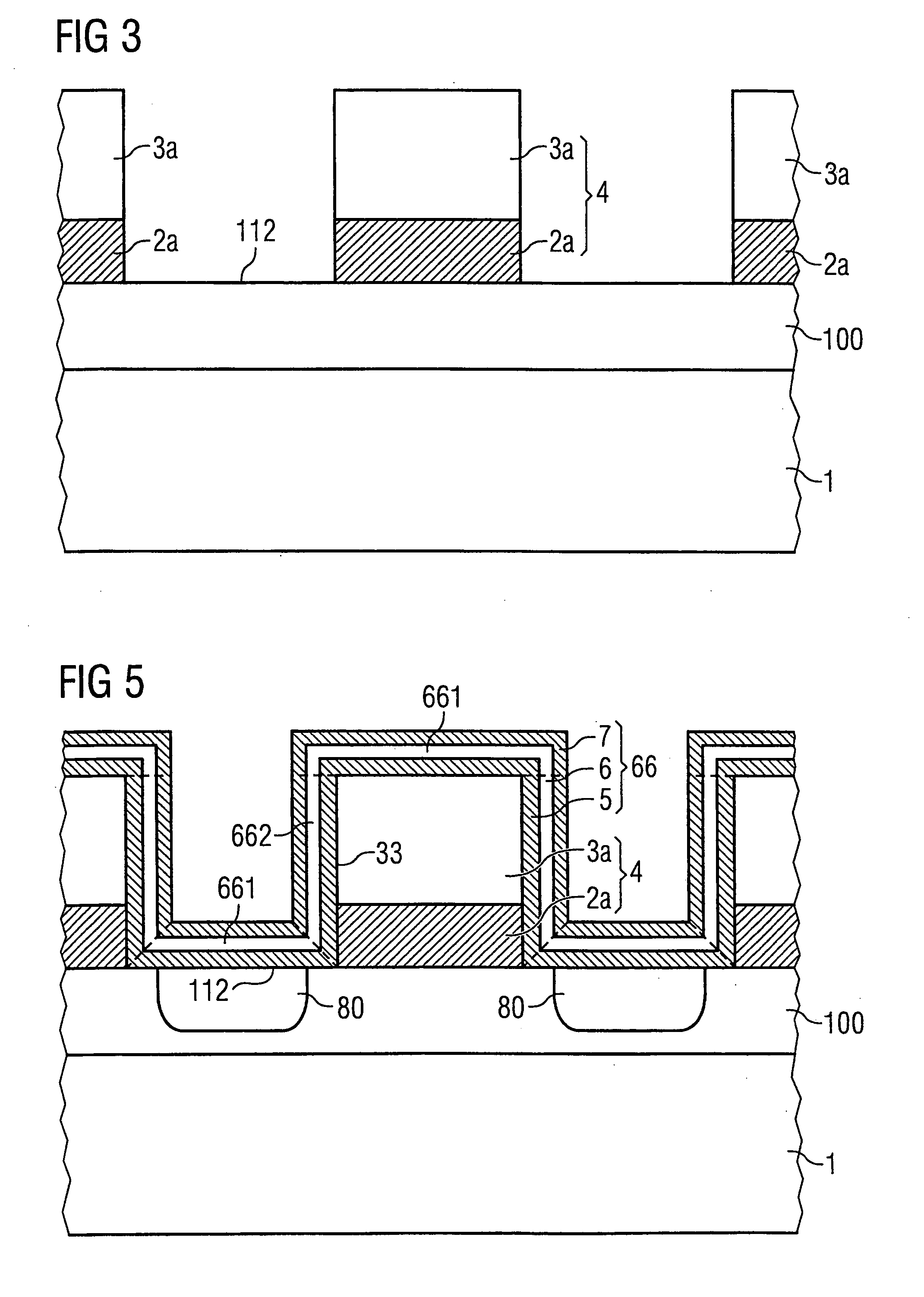
[0054] A production process of a semiconductor device comprises a plurality of steps to form patterned layers onto or into a substrate, which is in general monocrystalline silicon. A first embodiment production process of an inventive memory cell is described below and illustrated in FIGS. 1 to 14. These figures show cross-sections and top views of a small region of intermediate products of a semiconductor memory device.

[0055]FIG. 1 shows a cross-section of a region of an intermediate product of a semiconductor device. A semiconductor (e.g., silicon) substrate 1 is provided. A top surface 111 of the semiconductor substrate 1 is...


PUM


Abstract

Semiconductor Device And Method Of Producing A Semiconductor Device A semiconductor device comprises a memory cell (160) including a transistor body (150) having a top surface (111) and including a first doping area (10a) and a second doping area (10b) with a channel region (110) in between. The memory cell (160) further includes a gate electrode (3a) arranged above the channel region (110) and separated therefrom by a dielectric layer (2a). An oxide-nitride-oxide layer (66) has first portions (661) and second portions (662). The first portions (661) of the oxide-nitride-oxide layer (66) are arranged above at least parts of the first and second doping areas (10a, 10b) and are substantially parallel to the top surface (111) of the transistor body (150). The second portions (662) of the oxide-nitride-oxide layer (66) are adjacent to the gate electrode (3a) and extend in a direction not substantially parallel to the top surface (111) of the transistor body (150).

Description

TECHNICAL FIELD [0001] The present invention generally relates to a semiconductor memory device, more particularly to a multi-bit memory cell having a transistor body and an oxide-nitride-oxide layer, and further concerns a method of producing such a semiconductor memory device. BACKGROUND [0002] Portable devices, such as mobile phones, digital cameras and music players, comprise non-volatile memory units. These portable devices have become smaller in recent years, as have the respective memory units. It is assumed that the miniaturization of portable devices will proceed. The amount of data that can be stored in the non-volatile memory unit may increase to improve the performance of the device. As a result, for example, more music songs, photos or other data can be stored in smaller devices. [0003] Non-volatile memory units may be realized in different ways. Examples are read-only memory (ROM), programmable read-only memory (PROM), erasable programmable read-only memory (EPROM) and...

Claims


Application Information

Patent Timeline
IPC IPC(8): H01L29/788H01L21/336
CPCH01L27/115H01L27/11568H10B69/00H10B43/30
Inventor STRASSBURG, MATTHIASRIEDEL, STEPHAN
Owner QIMONDA
Why Eureka
Try Eureka