Light-emitting diode apparatus

a technology of light-emitting diodes and led apparatuses, which is applied in the direction of electrical apparatus, basic electric elements, and semiconductor devices, can solve the problems of disadvantageous reduction of emission efficiency, disadvantageous reduction of emission probability, and disadvantageous reduction of disadvantageous reduction of secondary light emitted from the package, so as to reduce the difference in intensity.

Inactive Publication Date: 2008-10-23
SANYO ELECTRIC CO LTD
View PDF7 Cites 98 Cited by
  • Summary
  • Abstract
  • Description
  • Claims
  • Application Information

AI Technical Summary

Benefits of technology

[0009]A light-emitting diode apparatus according to an aspect of the present invention comprises a light-emitting diode chip including an emission layer having a principal plane, and a package having a chip-arrangement surface on which the light-emitting diode chip is arranged, wherein primary light emitted from the principal plane of the emission layer has a pluralit

Problems solved by technology

Thus, in a case where the piezoelectric field exists in the GaInN quantum well, a quantum confined Stark effect shifting an energy level to a lower energy side, and emission probability is disadvantageously reduced since electrons and holes are pulled away and hence emission efficiency is disadvantageously reduced, as compared with a case where no electric field exists occurs.
Thus, it is disadvantageously difficult to reduce difference in th

Method used


Image

  • Light-emitting diode apparatus
  • Light-emitting diode apparatus
  • Light-emitting diode apparatus

Examples


first embodiment

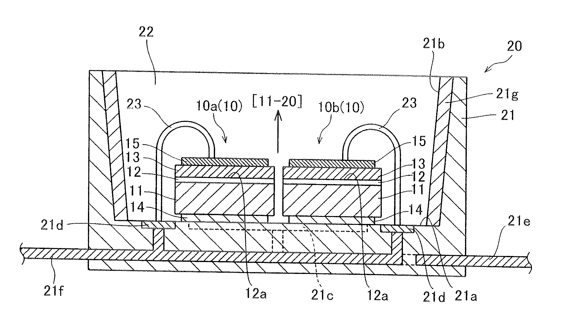
[0044]A structure of a light-emitting diode apparatus according to a first embodiment will be now described with reference to FIGS. 4 to 6.

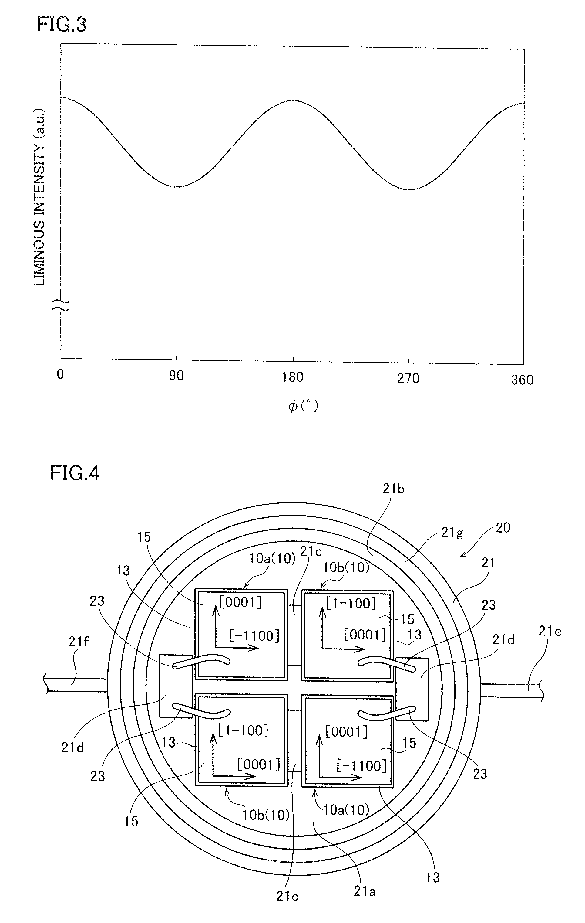
[0045]As shown in FIGS. 4 and 5, the light-emitting diode apparatus according to the first embodiment includes four light-emitting diode chips 10 and a package 20 in which the four light-emitting diode chips 10 are arranged.

[0046]Each light-emitting diode chip 10 is constituted by a wurtzite structure nitride-based semiconductor having a (11-20) plane as a principal plane. As shown in FIG. 4, outer shapes of the light-emitting diode chips 10 each include a square shape, a rectangular shape, a rhombus shape or a parallelogram shape or the like as viewed from an upper surface side.

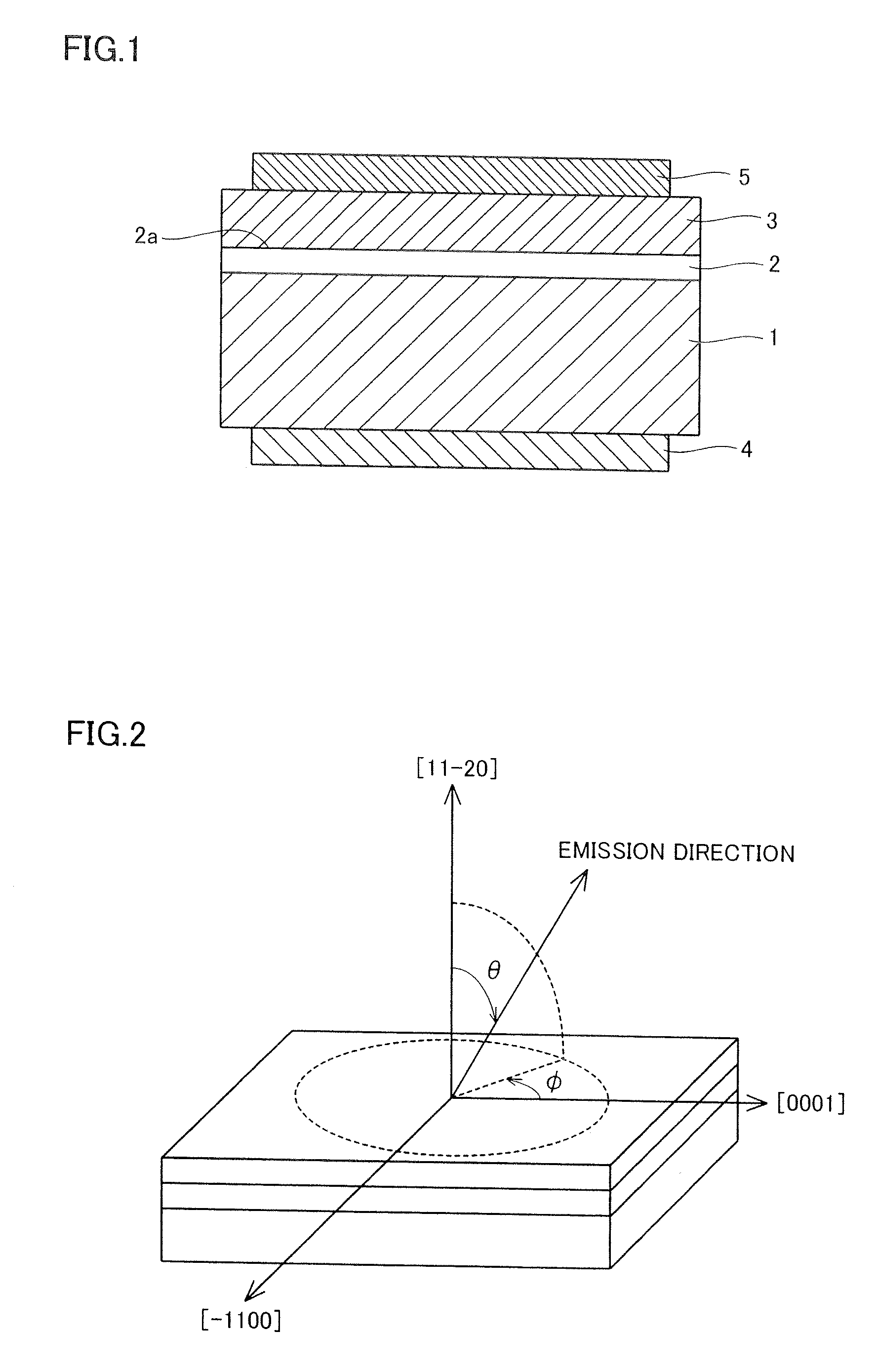
[0047]In each light-emitting diode chip 10, an emission layer 12 consisting of an MQW formed by stacking well layers (not shown) of Ga0.7In0.3N having a thickness of about 2 nm and barrier layers (not shown) of Ga0.9In0.1N is formed on an n-type GaN substrate 11 having a ...

second embodiment

[0055]Referring to FIGS. 8 and 9, a reflective side surface of a package is formed with a shape reducing difference in the intensity of secondary light emitted from the package according to variation in the in-plane azimuth angle of a chip-arrangement surface in a light-emitting diode apparatus according to a second embodiment, dissimilarly to the light-emitting diode apparatus according to the first embodiment.

[0056]The light-emitting diode apparatus according to the second embodiment includes one light-emitting diode chip 30 and a package 40 in which the one light-emitting diode chip 30 is arranged, as shown in FIGS. 8 and 9.

[0057]The light-emitting diode chip 30 is constituted by a wurtzite structure nitride-based semiconductor having a (1-100) plane as a principal plane. As shown in FIG. 8, the light-emitting diode chip 30 is formed in a square shape having a size of about 300 μm×about 300 μm as viewed from an upper surface side.

[0058]In the light-emitting diode chip 30, an emis...

third embodiment

[0066]Referring to FIGS. 10 and 11, a corrugatedly shaped portion extending in a prescribed direction is formed on a light-emission surface (upper surface) of a light-emitting diode chip according to a third embodiment in order to reduce difference in the luminous intensity of secondary light emitted from a package (light-emitting diode chip).

[0067]The light-emitting diode apparatus according to the third embodiment includes one light-emitting diode chip 50 and a package 60 in which the one light-emitting diode chip 50 is arranged, as shown in FIGS. 10 and 11.

[0068]The light-emitting diode chip 50 is constituted by a wurtzite structure nitride-based semiconductor having a (11-24) plane as a principal plane. In the light-emitting diode chip 50, an emission layer 52 consisting of an MQW formed by stacking well layers (not shown) of Ga0.7In0.3N having a thickness of about 2 nm and barrier layers (not shown) of Ga0.9In0.1N is formed on an n-type GaN layer 51, as shown in FIG. 11. A p-ty...


PUM


Abstract

In a light-emitting diode apparatus, light emitted from a principal plane of an emission layer has a plurality of unequal luminous intensities depending on the in-plane azimuth angle of the principal plane of the emission layer, and at least one of a light-emitting diode chip and a package has a structure of reducing difference in the intensity of light emitted from the package according to variation in the in-plane azimuth angle of a chip-arrangement surface.

Description

CROSS-REFERENCE TO RELATED APPLICATIONS[0001]The first priority application number JP2006-268825, Light-Emitting Diode Apparatus, Sep. 29, 2006, Masayuki Hata, and the second priority application number JP2007-233391, Light-Emitting Diode Apparatus, Sep. 7, 2007, Masayuki Hata, upon which this patent application is based are hereby incorporated by reference.BACKGROUND OF THE INVENTION[0002]1. Field of the Invention[0003]The present invention relates to a light-emitting diode (LED) apparatus, and more particularly it relates to an LED apparatus comprising a light-emitting diode chip.[0004]2. Description of the Background Art[0005]In a light-emitting diode apparatus comprising a light-emitting diode chip, it is known in general that a large piezoelectric field is formed in a direction perpendicular to a quantum well (QW) plane in a GaInN QW prepared on a GaN C plane (0001) substrate. Thus, in a case where the piezoelectric field exists in the GaInN quantum well, a quantum confined Sta...

Claims


Application Information

Patent Timeline
IPC IPC(8): H01L33/00H01L33/32H01L33/06H01L33/54H01L33/56H01L33/60H01L33/62
CPCH01L25/0753H01L33/20H01L33/60H01L24/05H01L2224/48091H01L2224/73265H01L2224/04042H01L2924/00H01L2924/181H01L2924/12041H01L2924/00014
Inventor HATA, MASAYUKI
Owner SANYO ELECTRIC CO LTD
Why Eureka
Try Eureka