Capacitor Unit and Method of Forming the Same

a technology of capacitors and units, applied in the field of capacitor units, can solve the problems of reducing the size of analog circuits, reducing the size of digital circuits incorporated into systems-on-chips (socs), and substantially reducing the size of passive elements such as capacitors. the effect of reducing the first coefficient and the second coefficien

Active Publication Date: 2008-10-30
SAMSUNG ELECTRONICS CO LTD
View PDF3 Cites 13 Cited by
  • Summary
  • Abstract
  • Description
  • Claims
  • Application Information

AI Technical Summary

Problems solved by technology

The size of digital circuits incorporated into systems-on-chip (SOCs) has rapidly decreased; however, the size of analog circuits has not decreased very much.
This is in large part attributable to the inability to substantially reduce the size of passive elements such as capacitors.
Additionally, even the polysilicon layer doped with the impurities has a depletion area, so that the VCC may not be sufficiently decreased.
Thus, the capacitor having the PIP structure is not suitable for an analog capacitor, which is employed in an analog-to-digital converter (ADC), a radio frequency (RF) device, a complementary metal-oxide semiconductor (CMOS) image sensor (CIS), etc.
However, even the capacitor having the MIM structure does not have a sufficiently small VCC, and reducing the VCC may be needed in order to serve as an analog capacitor having high precision.

Method used


Image

  • Capacitor Unit and Method of Forming the Same
  • Capacitor Unit and Method of Forming the Same
  • Capacitor Unit and Method of Forming the Same

Examples


Embodiment Construction

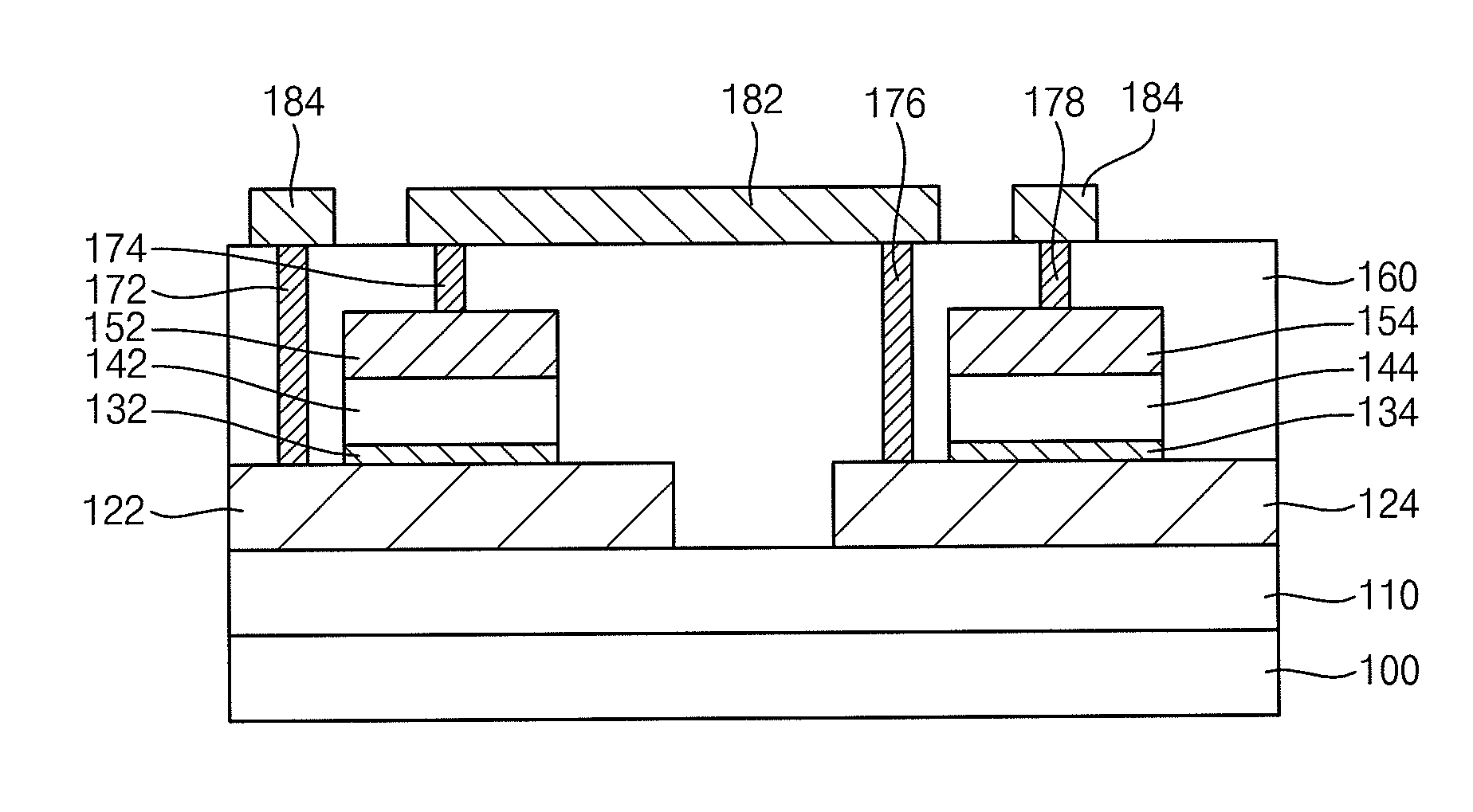
[0045]Exemplary embodiments of the present invention are described more fully hereinafter with reference to the accompanying drawings. The present invention may, however, be embodied in many different forms and should not be construed as limited to the exemplary embodiments set forth herein. In the drawings, the sizes and relative sizes of layers and regions may be exaggerated for clarity.

[0046]It will be understood that when an element or layer is referred to as being “on,”“connected to” or “coupled to” another element or layer, it can be directly on, connected or coupled to the other element or layer or intervening elements or layers may be present. In contrast, when an element is referred to as being “directly on,”“directly connected to” or “directly coupled to” another element or layer, there are no intervening elements or layers present. Like numerals refer to like elements throughout. As used herein, the term “and / or” includes any and all combinations of one or more of the ass...


PUM


Abstract

A capacitor unit includes a first capacitor and a second capacitor. The first capacitor includes a first lower electrode, a first dielectric layer pattern and a first upper electrode sequentially stacked. The first capacitor includes a first control layer pattern for controlling a voltage coefficient of capacitance (VCC) of the first capacitor between the first lower electrode and the first dielectric layer pattern. The second capacitor includes a second lower electrode, a second dielectric layer pattern and a second upper electrode sequentially stacked. The second lower electrode is electrically connected to the first upper electrode, and the second upper electrode is electrically connected to the second lower electrode. The second capacitor includes a second control layer pattern for controlling a VCC of the second capacitor between the second lower electrode and the second dielectric layer pattern.

Description

CROSS-REFERENCE TO RELATED APPLICATIONS[0001]This application claims priority under 35 U.S.C. § 119 to Korean Patent Application No. 10-2007-0040611, filed on Apr. 26, 2007 in the Korean Intellectual Property Office (KIPO), the contents of which are herein incorporated by reference in their entirety.BACKGROUND OF THE INVENTION[0002]1. Technical Field[0003]The present invention relates to a capacitor unit and more particularly, to a capacitor unit and a method of forming the same.[0004]2. Discussion of the Related Art[0005]The size of digital circuits incorporated into systems-on-chip (SOCs) has rapidly decreased; however, the size of analog circuits has not decreased very much. This is in large part attributable to the inability to substantially reduce the size of passive elements such as capacitors. Thus reducing the size of capacitors is important to achieve a high degree of integration in a semiconductor device.[0006]The capacitance of a capacitor is proportional to a dielectric ...

Claims


Application Information

Patent Timeline
Patent Type & Authority Applications(United States)
IPC IPC(8): H01L29/66H01L21/20
CPCH01G4/33H01G4/38H01L28/65Y10S438/957H10B99/00H10B12/00
Inventor PARK, JUNG-MINWON, SEOK-JUNSONG, MIN-WOOKIM, WEON-HONG
Owner SAMSUNG ELECTRONICS CO LTD
Why Eureka
Try Eureka