Scribe line layout design

a scribe line and layout technology, applied in the direction of semiconductor devices, semiconductor/solid-state device details, electrical devices, etc., can solve the problems of cracking silicon crystals, cracking the physical structure of the die, and cracking the silicon crystals, so as to reduce the damage done during the dicing process

Active Publication Date: 2008-10-30
TAIWAN SEMICON MFG CO LTD
View PDF67 Cites 58 Cited by
  • Summary
  • Abstract
  • Description
  • Claims
  • Application Information

AI Technical Summary

Benefits of technology

[0006]These and other problems are generally solved or circumvented, and technical advantages are generally achieved, by preferred embodiments of the present invention which help to prevent cracking and delamination of semiconductor dies when the dies are cut from the wafer.
[0010]The metal plates and grooves located within the scribe lines work to release pressure caused by the sawing of the wafer during the dicing process. By relieving this pressure, the damage done during the dicing process can be reduced, and fewer die will be rendered useless.

Problems solved by technology

Unfortunately, the physical process of sawing the wafer may damage the physical structure of the dies, especially around the corners of the die.
For example, the saw could crack the silicon crystal, and these cracks could then propagate through the dies.
Damage such as this would render the dies unusable and decreases the yield.
This reduction in size is expected to exasperate the problem with damage created by separating the die, and makes this problem even more critical.

Method used


Image

  • Scribe line layout design
  • Scribe line layout design
  • Scribe line layout design

Examples


Embodiment Construction

[0018]The making and using of the presently preferred embodiments are discussed in detail below. It should be appreciated, however, that the present invention provides many applicable inventive concepts that can be embodied in a wide variety of specific contexts. The specific embodiments discussed are merely illustrative of specific ways to make and use the invention, and do not limit the scope of the invention.

[0019]The present invention will be described with respect to preferred embodiments in a specific context, namely a scribe line layout design to prevent damage during dicing operations. The invention may also be applied, however, to other dicing operations where cracking and defects are a problem.

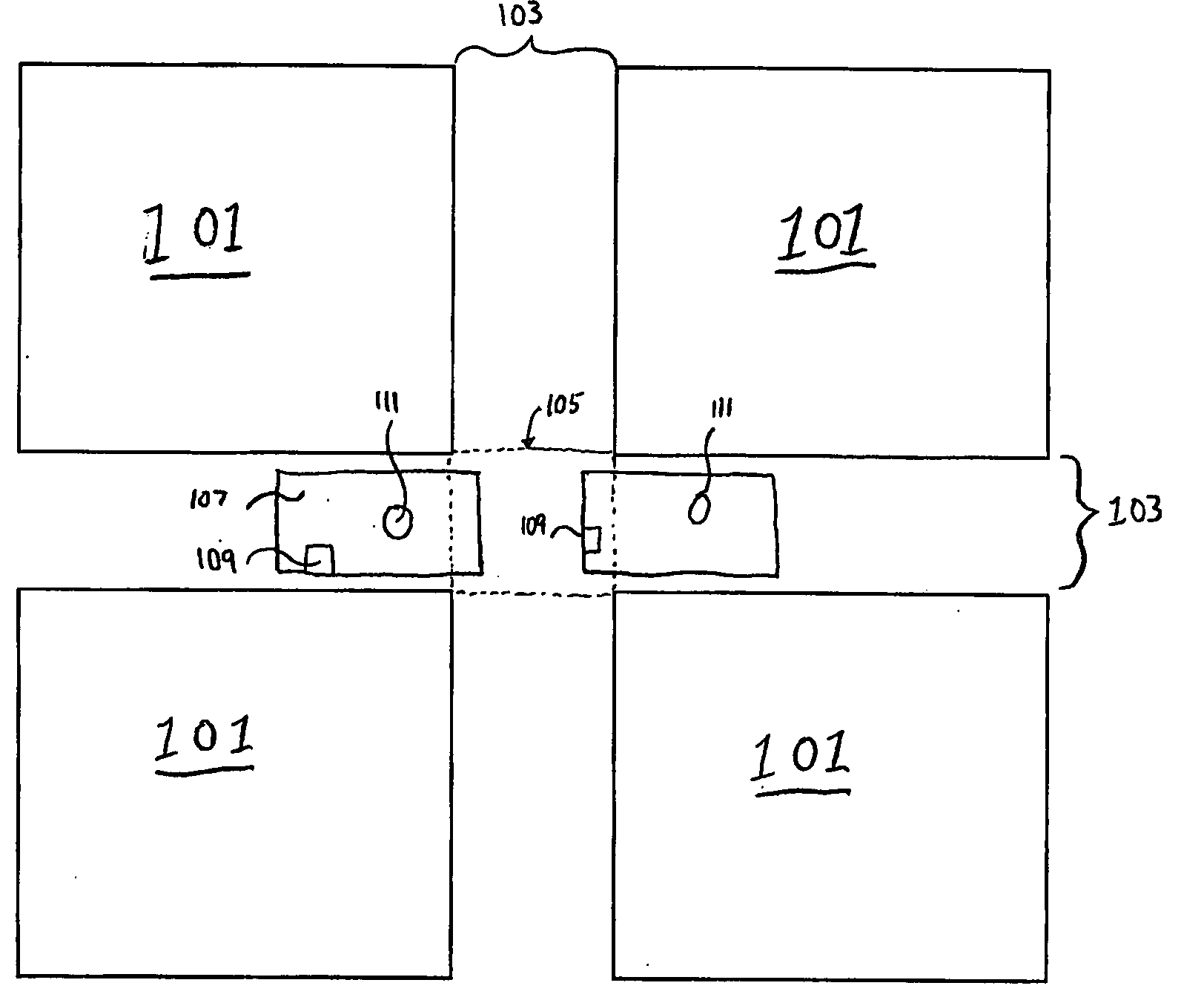
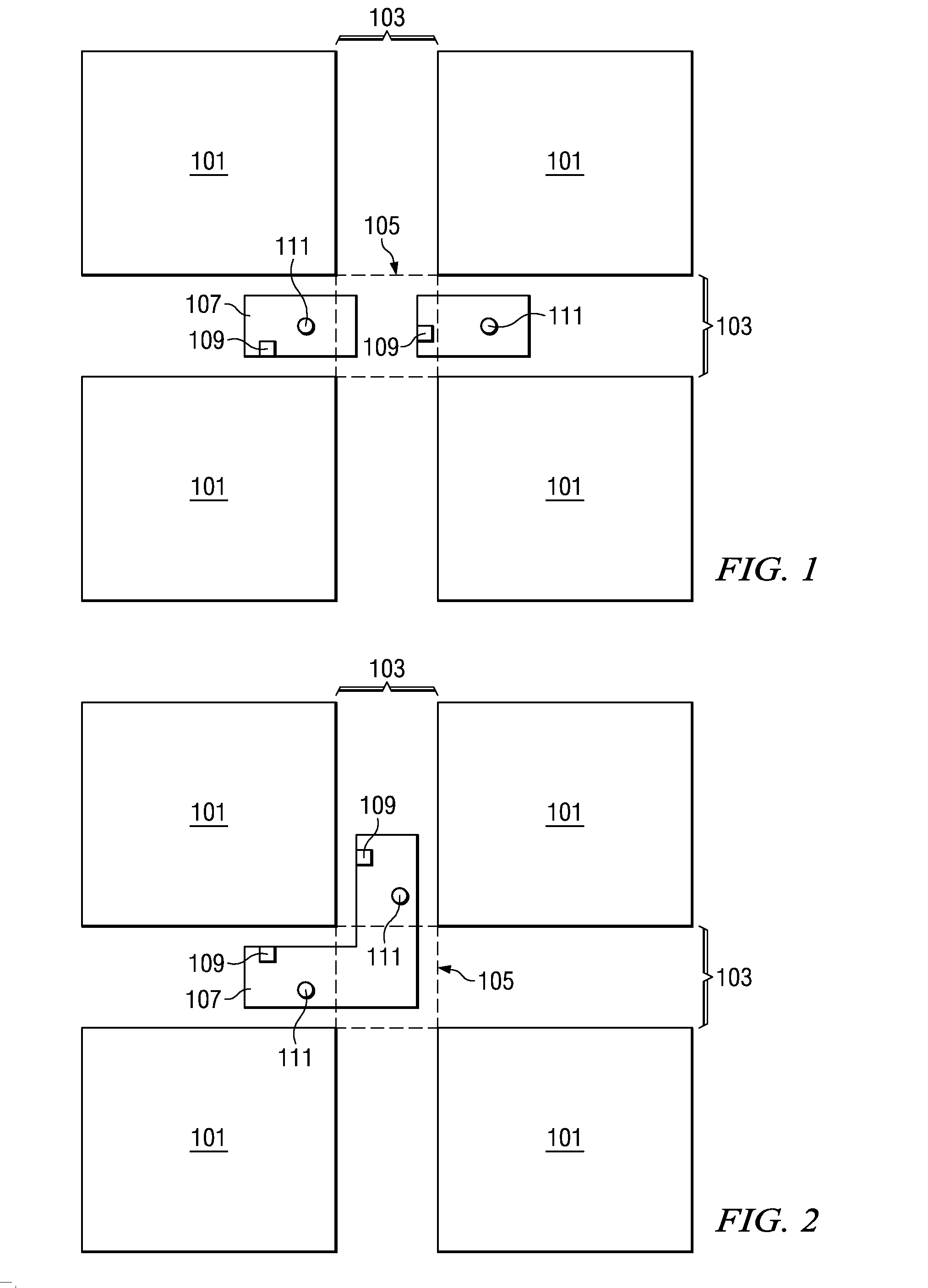
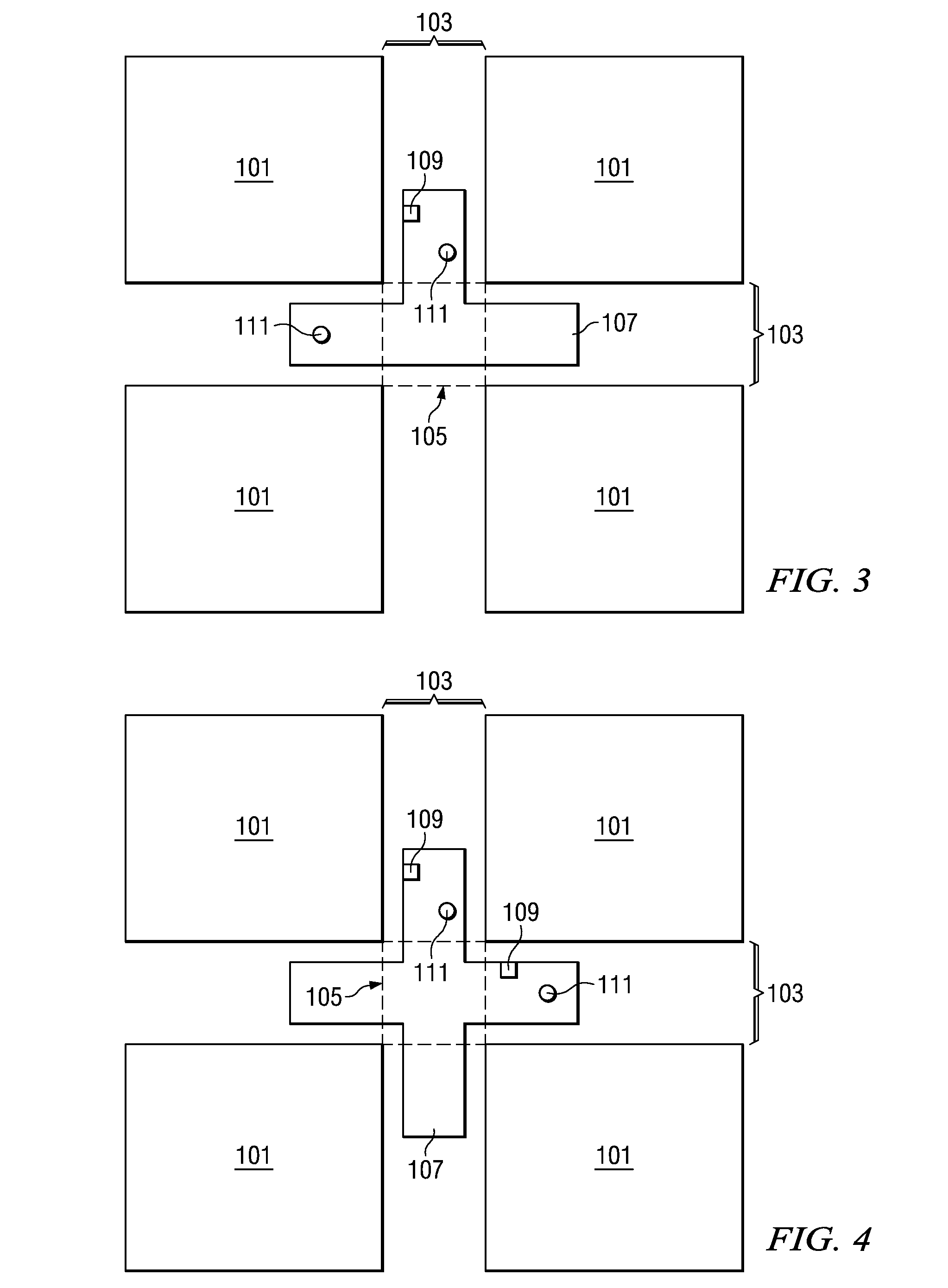
[0020]With reference now to FIG. 1, there is shown an embodiment of the present invention comprising a plurality of individual dies 101, wherein each die 101 includes a substrate (not shown) having electronic devices formed thereon as is known in the art. The substrate is typically c...


PUM


Abstract

A scribe line layout design to reduce the damage caused by sawing the wafer is presented. An embodiment comprises metal plates located within the scribe lines and at least partially within the junctions of the scribe lines. Each of these metal plates has one or more slots to help relieve the pressure. Alternatively, instead of metal plates, grooves that may be filled with metal could be placed into the scribe lines. These metal plates could also be used concurrently with a seal ring for better protection during sawing.

Description

TECHNICAL FIELD[0001]The present invention relates generally to a system and method for manufacturing semiconductor devices and, more particularly, to improving the quality of dicing when dicing semiconductor dies.BACKGROUND[0002]In the manufacturing of semiconductor devices, the first step is the formation of a silicon wafer. These wafers are manufactured by growing a single silicon crystal. This single crystal is then processed through such steps as the evaluation and testing of the physical properties of the crystal, grinding the crystal to a desired diameter, sawing the single silicon crystal into wafers, marking the wafers with a laser, grinding the wafers to a specified thickness, edge rounding, etching away damaged areas, and polishing the surface.[0003]These wafers are then processed into individual dies by the deposition and placement of structures and layers onto the wafers. Once each of the dies has been tested for functionality, the dies are separated from the wafer usin...

Claims


Application Information

Patent Timeline
Patent Type & Authority Applications(United States)
IPC IPC(8): H01L23/544
CPCH01L23/544H01L23/585H01L2223/5442H01L2223/5446H01L2924/0002H01L2924/00
Inventor LEE, HSIN-HUILII, MIRNG-JIJENG, SHIN-PUUHOU, SHANG-YUN
Owner TAIWAN SEMICON MFG CO LTD
Why Eureka
Try Eureka