Method of fabricating a flash memory device

Inactive Publication Date: 2008-10-30
SK HYNIX INC
View PDF33 Cites 10 Cited by
  • Summary
  • Abstract
  • Description
  • Claims
  • Application Information

AI Technical Summary

Benefits of technology

[0010]The present invention is directed to a method of fabricating a flash memory device. After an isolation trench is formed, a bottom surface and sidewalls of the trench are gap-filled with a High Aspect Ratio Process (HARP) film having a favorable step coverage. A wet etch process is performed causing the HARP film to remain on the sidewalls of a tunnel dielectric layer, such that a wing spacer is formed. Thus, the tunnel dielectric layer can be protected and an interference phenomenon can be reduced because a control gate to be formed subsequently is located between floating gates.

Problems solved by technology

The state of the cell is changed due to this interference phenomenon, which results in an increased failure rate and a low yield.
If the flash memory device is fabricated by the SA-STI process as described above, interference may occur between the first polysilicon films because the isolation layer is formed between the first polysilicon film, serving as a floating gate, and a neighboring first polysilicon film.

Method used


Image

  • Method of fabricating a flash memory device
  • Method of fabricating a flash memory device
  • Method of fabricating a flash memory device

Examples


Embodiment Construction

[0020]A specific embodiment according to the present invention is described with reference to the accompanying drawings.

[0021]FIGS. 3 to 11 are cross-sectional views illustrating a method of fabricating a flash memory device according to an embodiment of the present invention.

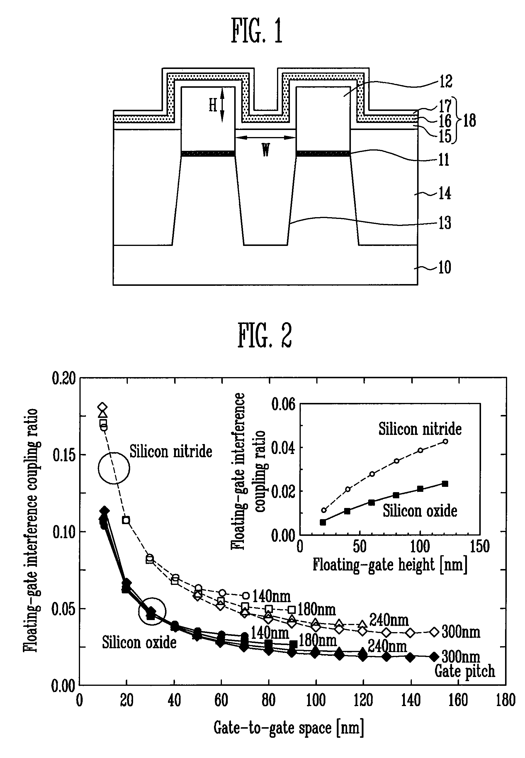
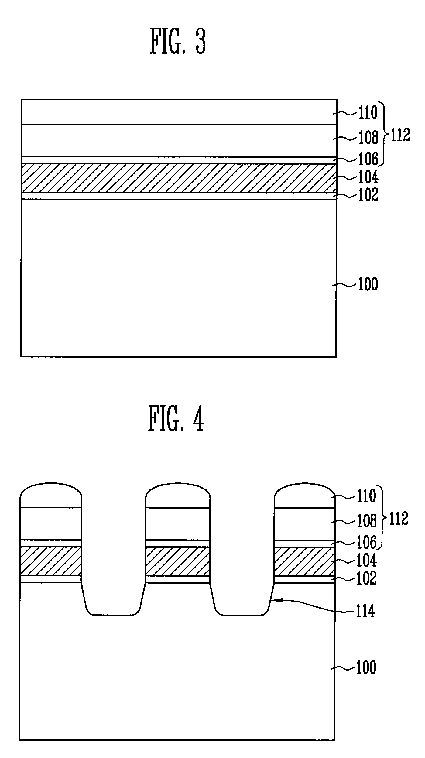
[0022]Referring to FIG. 3, a tunnel dielectric layer 102, an electron storage layer 104 and an isolation mask 112 are sequentially formed over a semiconductor substrate 100. The isolation mask 112 may have a stack structure of a buffer oxide layer 106, a nitride layer 108, and a hard mask 110. The hard mask 110 may be formed of a nitride matter, an oxide matter, SiON or amorphous carbon. The electron storage layer 104 forms a floating gate of the flash memory device, and may be formed of polysilicon or a silicon nitride layer. Alternatively, the electron storage layer 104 may be formed of any material capable of storing electrons.

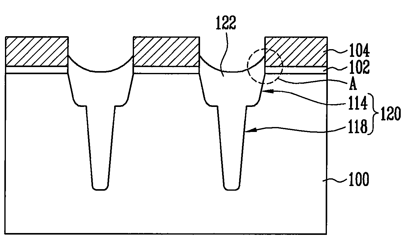
[0023]Referring to FIG. 4, the isolation mask 112, the electron storage layer 104,...


PUM


Abstract

In a method of fabricating a flash memory device, after an isolation trench is formed, a bottom surface and sidewalls of the trench are gap-filled with a HARP film having a favorable step coverage. A wet etch process is performed such that the HARP film remains on the sidewalls of a tunnel dielectric layer, thereby forming a wing spacer. Accordingly, the tunnel dielectric layer can be protected and an interference phenomenon can be reduced because a control gate to be formed subsequently is located between floating gates.

Description

CROSS-REFERENCES TO RELATED APPLICATIONS[0001]The present application claims priority to Korean patent application number 10-2007-40332, filed on Apr. 4, 2007, which is incorporated by reference in its entirety.BACKGROUND OF THE INVENTION[0002]The present invention relates to flash memory devices and, more particularly, to a method of fabricating a flash memory device in which an interference phenomenon between floating gates can be reduced.[0003]A NAND flash memory device includes a plurality of cells for storing data, which are connected in series to form a string. A drain select transistor and a source select transistor are formed between a cell string and a drain, and the cell string and a source, respectively. In a cell of the NAND flash memory device, a stack gate of a tunnel oxide layer, a floating gate, a dielectric layer, and a control gate is formed in a specific region on a semiconductor substrate. A junction is formed at both sides of the gate.[0004]In the NAND flash mem...

Claims


Application Information

Patent Timeline
IPC IPC(8): H01L21/76
CPCH01L27/11521H10B41/30H01L21/28141H01L21/31051H01L21/76229H01L21/76838
Inventor KIM, SUK JOONGCHO, WHEE WONKIM, JUNG GEUNMYUNG, SEONG HWAN
Owner SK HYNIX INC
Why Eureka
Try Eureka