

Method for making a circuit board and multi-layer substrate with plated through holes
- Summary
- Abstract
- Description
- Claims
- Application Information
AI Technical Summary
Benefits of technology
Problems solved by technology
Method used
Image

Examples
first embodiment
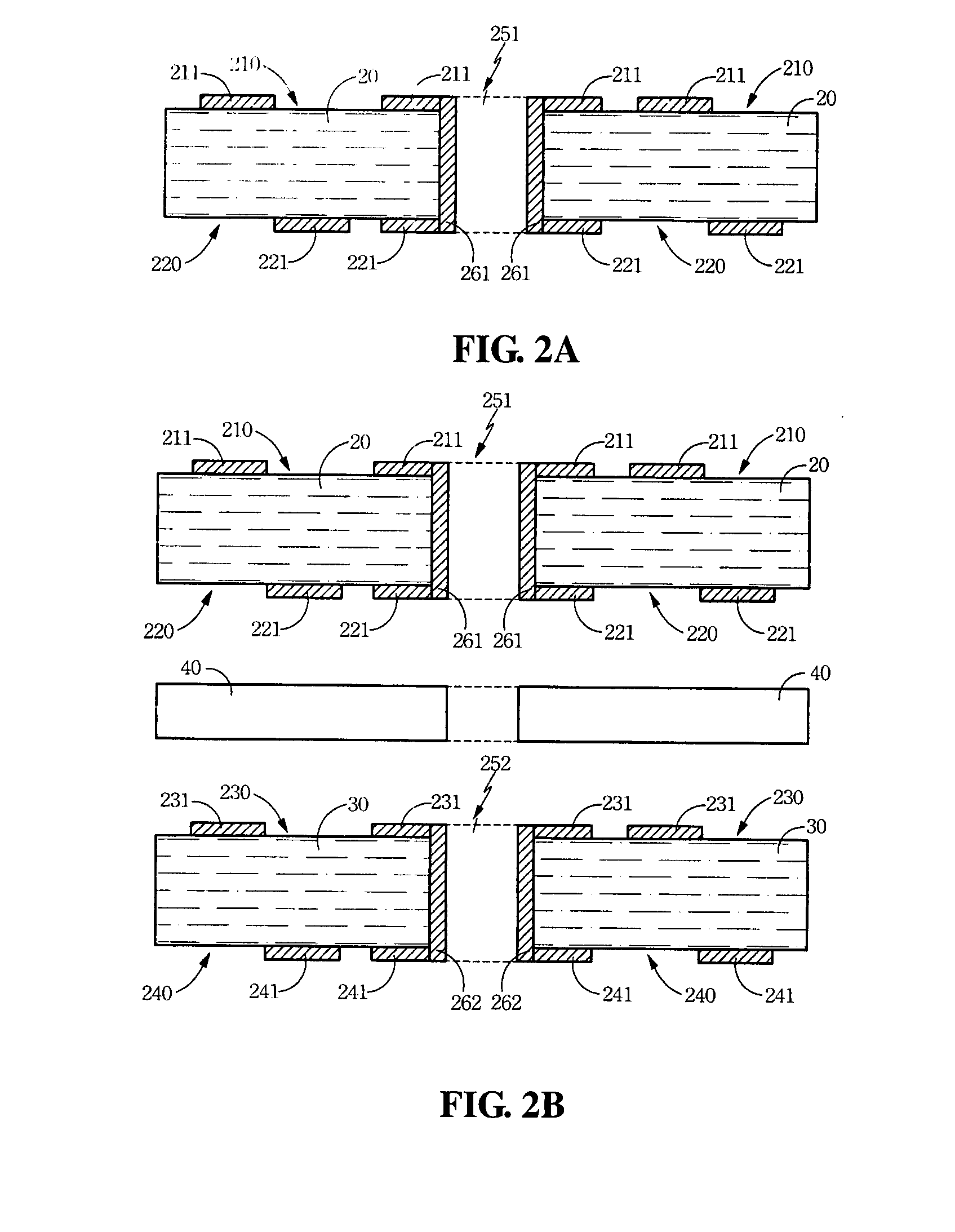
[0028]Referring to FIGS. 2A to 2F, they depict a method for making a circuit board according to the present invention. Referring to FIG. 2A, a first substrate 20 is provided and includes a first circuit layer 211 formed on a first surface 210 and a second circuit layer 221 formed on a second surface 220, wherein the second surface 220 is opposite to the first surface 210. The first surface 210 and the second surface 220 are the upper and lower surfaces of first substrate 20 respectively.
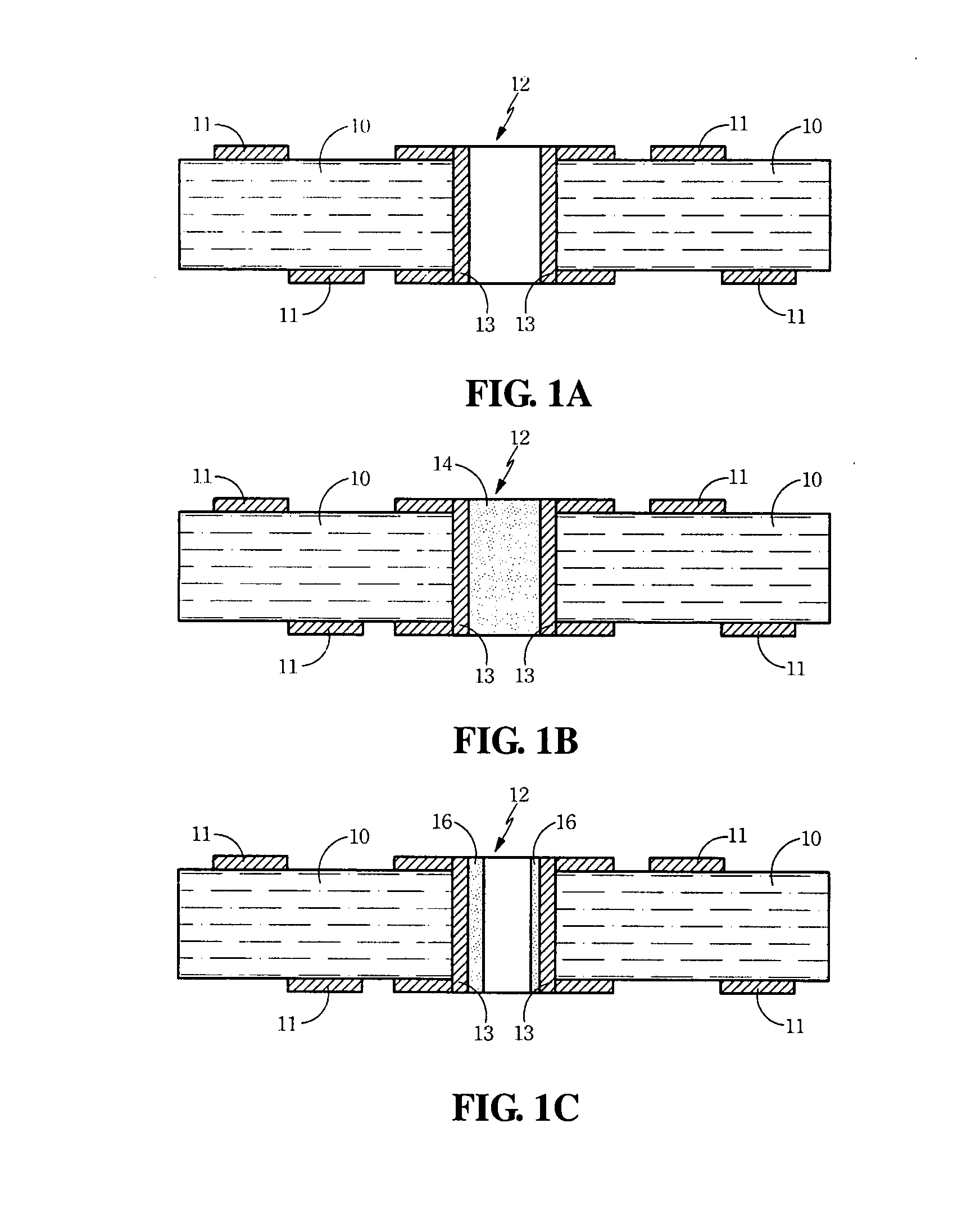
[0029]In addition, at least one first via 251 passes through the first surface 210 and the second surface 220, and a first metal layer 261 is formed on a side wall of the first via 251 for electrically connecting the first circuit layer 211 to the second circuit layer 221. In other words, the first metal layer 261 provides an electrical channel between the first circuit layer 211 and the second circuit layer 221. The first via 251 is formed by using a mechanical drilling process or a laser drilling p...
second embodiment
[0053]In addition, the circuit layer 30 in the second embodiment can be processed by the electrophoretic deposition process if necessary, whereby the insulating film 280 is also formed on the second metal layer 262. Then, the third metal layer 263 formed on the insulating film 280 can electrically connects the first circuit layer 211 to the fourth circuit layer 241.
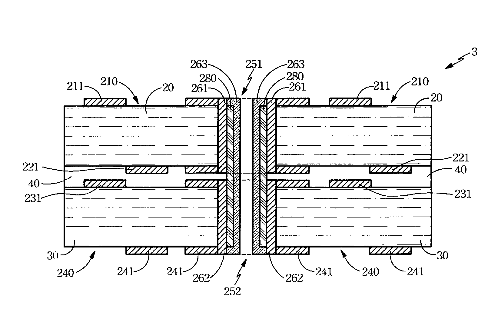
[0054]FIGS. 2F and 3C respectively show the multi-layer substrate 3 with plated through holes of the present invention. The multi-layer substrate 3 includes the first substrate 20, the first metal layer 261, the second substrate 30, the second metal layer 262, the insulating film 280 and the third metal layer 263.
[0055]The first substrate 20 includes the first circuit layer 211 formed on the first surface 210 and the second circuit layer 221 formed on the second surface 220, wherein the second surface 220 is opposite to the first surface 210. The first substrate 20 further includes at least one first via 251 passing throu...
PUM
| Property | Measurement | Unit |
|---|---|---|
| Time | aaaaa | aaaaa |
| aaaaa | aaaaa |
Abstract
Description
Claims
Application Information