Magnetic sensor using giant magnetoresistive elements and method for manufacturing the same
a technology of magnetoresistive elements and magnetic sensors, applied in the field of magnetic sensors, can solve the problems of imbalanced bridge circuits of magnetic sensors, difficult to miniaturize the magnetic sensors (chips) sufficiently, and difficult to generate such magnetic fields oriented in different directions. , to achieve the effect of easy and efficient formation
- Summary
- Abstract
- Description
- Claims
- Application Information
AI Technical Summary
Benefits of technology
Problems solved by technology
Method used
Image
Examples
first embodiment
Structure of Magnetic Sensor
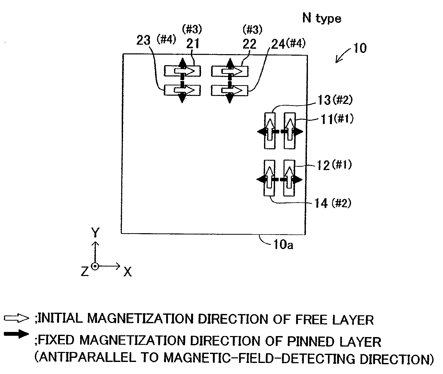
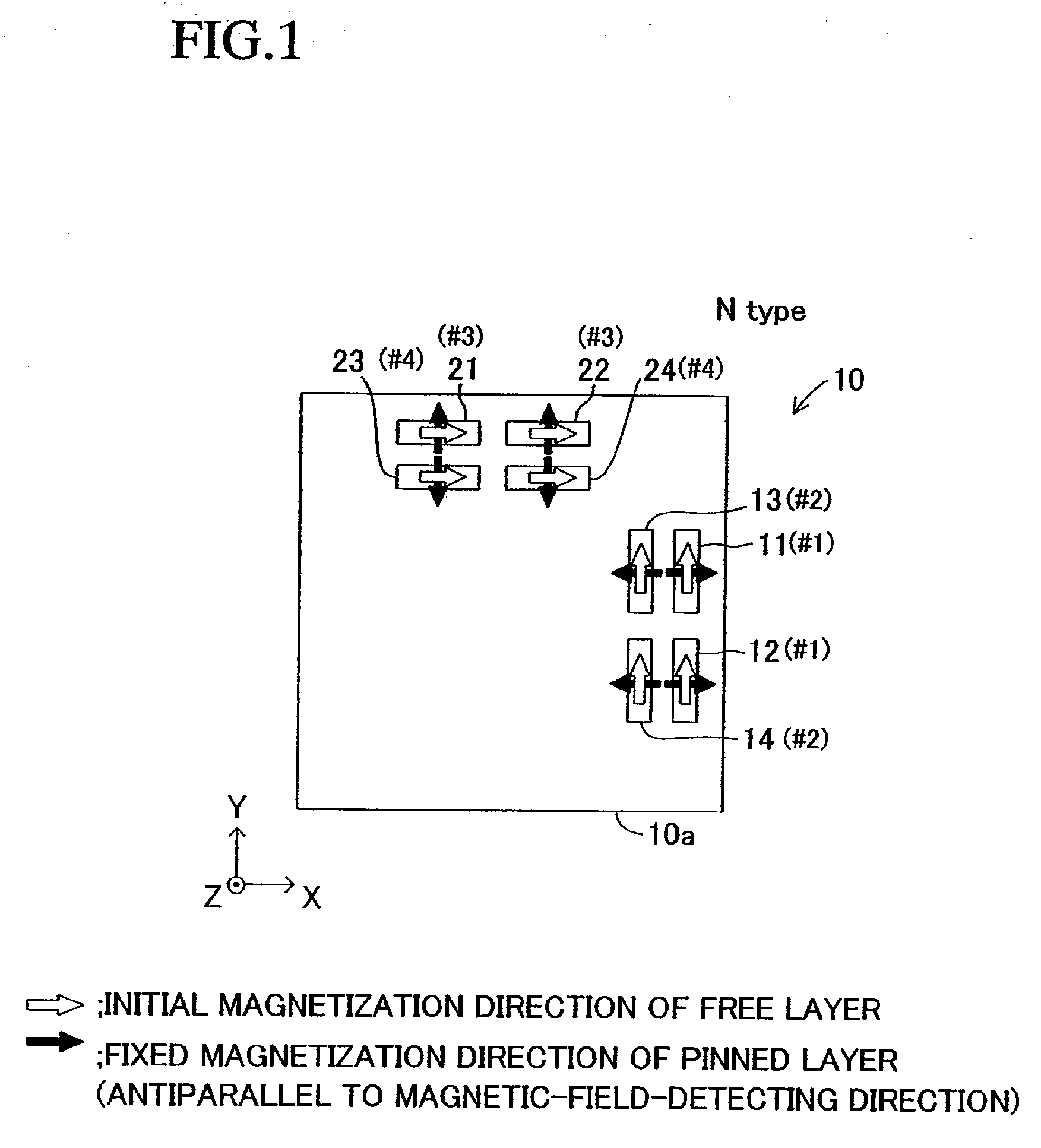
[0271]FIG. 1 is a plan view of a magnetic sensor 10 according to a first embodiment of the present invention. The magnetic sensor 10 includes a single substrate (monolithic chip) 10a and a total of eight giant magnetoresistive elements 11 to 14 and 21 to 24. The magnetic sensor 10 is referred to as an “N-type magnetic sensor 10” for the sake of convenience.
[0272]The substrate 10a is a thin silicon plate made of silicon. In plan view, the substrate 10a has a rectangular (substantially square) shape defined by four edges extending along mutually orthogonal X-axis and Y-axis. The substrate 10a has a small thickness along the Z-axis orthogonal to the X- and Y-axes.
[0273]Giant magnetoresistive elements 11, 12, 21, and 22 are conventional GMR elements. The other giant magnetoresistive elements 13, 14, 23, and 24 are elements (hereinafter referred to as “SAF elements” for the sake of convenience, described in detail later) having a synthetic spin-valve film incl...
second embodiment
[0387]A magnetic sensor according to a second embodiment of the present invention will now be described. As shown in FIG. 30, a magnetic sensor 50 includes a single substrate 50a, conventional GMR elements 51G to 54G, SAF elements 61S to 64S, conventional GMR elements 71G to 74G, and SAF elements 81S to 84S.
[0388]The substrate 50a is a thin silicon plate having the same shape as the substrate 10a.
[0389]The conventional GMR elements 51G to 54G and 71G to 74G each have the same structure as the foregoing conventional GMR element 11. The SAF elements 61S to 64S and 81S to 84S each have the same structure as the foregoing SAF element 13. The spin-valve film of each element (e.g., the thickness of the layers of the spin-valve film) is designed so that the elements have the same resistance if magnetic fields with an identical intensity are applied to the elements in their respective magnetic-field-detecting directions, and so that the resistances of the elements vary by the same amount (...
third embodiment
[0440]A magnetic sensor according to a third embodiment of the present invention is different from the magnetic sensor 10 of the first embodiment shown in FIG. 1 only in that a group comprising one conventional GMR element (for example, the conventional GMR element 11) and one SAF element (for example, the SAF element 13) in which the conventional GMR element and the SAF element is disposed closely to each other is replaced by a group shown in either FIG. 39 or 40. The following description will illustrate the difference.
[0441]Specifically, in the magnetic sensor of the third embodiment, a first element group constituted of the conventional GMR element 11 and the SAF element 13 in the magnetic sensor 10 of the first embodiment is replaced by an element group 91 shown in FIG. 39. The element group 91 is disposed in a position corresponding to the position on the substrate 10a shown in FIG. 1 where the first element group is disposed.
[0442]The element group 91 includes four convention...
PUM
 Abstract
Description
Claims
Application Information


