Process for producing silicon compound

a technology of silicon compound and process, applied in the direction of metal silicide, vacuum evaporation coating, coating, etc., can solve the problems of large number of steps, and defect in device manufacturing, so as to achieve easy and efficient formation, free from deterioration, and the effect of efficient production of the compound

Inactive Publication Date: 2010-08-17
CANON ANELVA CORP
View PDF16 Cites 2 Cited by
  • Summary
  • Abstract
  • Description
  • Claims
  • Application Information

AI Technical Summary

Benefits of technology

[0029]According to the present invention, a desired silicon compound is produced by a specific CVD apparatus which utilizes the etching reaction of the member to be etched, the adsorption reaction of the precursor formed by the etching reaction, and the reduction reaction of the adsorbed precursor. Thus, the silicon compound can be produced at a low temperature. Consequently, if a gate film or the like of a transistor is to be produced, in particular, a thin film of the desired silicon compound can be produced, with its characteristics free from deterioration. If a Si interface and SiO2 are coexistent, in particular, NiSi can be selectively grown at the Si interface. Thus, a source electrode and a drain electrode of an MOS transistor can be easily and efficiently formed.
[0030]Furthermore, unlike the conventional technologies, there is no need for a separate step, such as removal of the unnecessary portion, after heat treatment is completed. Accordingly, the production of the compound concerned can be performed efficiently.

Problems solved by technology

However, Ni which has been deposited for the formation of NiSi, or an impurity with which a semiconductor has been doped, may be diffused to cause defects in device manufacturing, or deterioration of characteristics.
Such a process involves the problems that the number of steps is large, and the treating temperature is still high.
The higher the treating temperature, the more likely it is that problems will occur, such as the degradation of performance of the MOS transistor due to the diffusion of the doped impurity or the deterioration of insulation in the gate insulating film 05.

Method used


Image

  • Process for producing silicon compound
  • Process for producing silicon compound
  • Process for producing silicon compound

Examples


first example

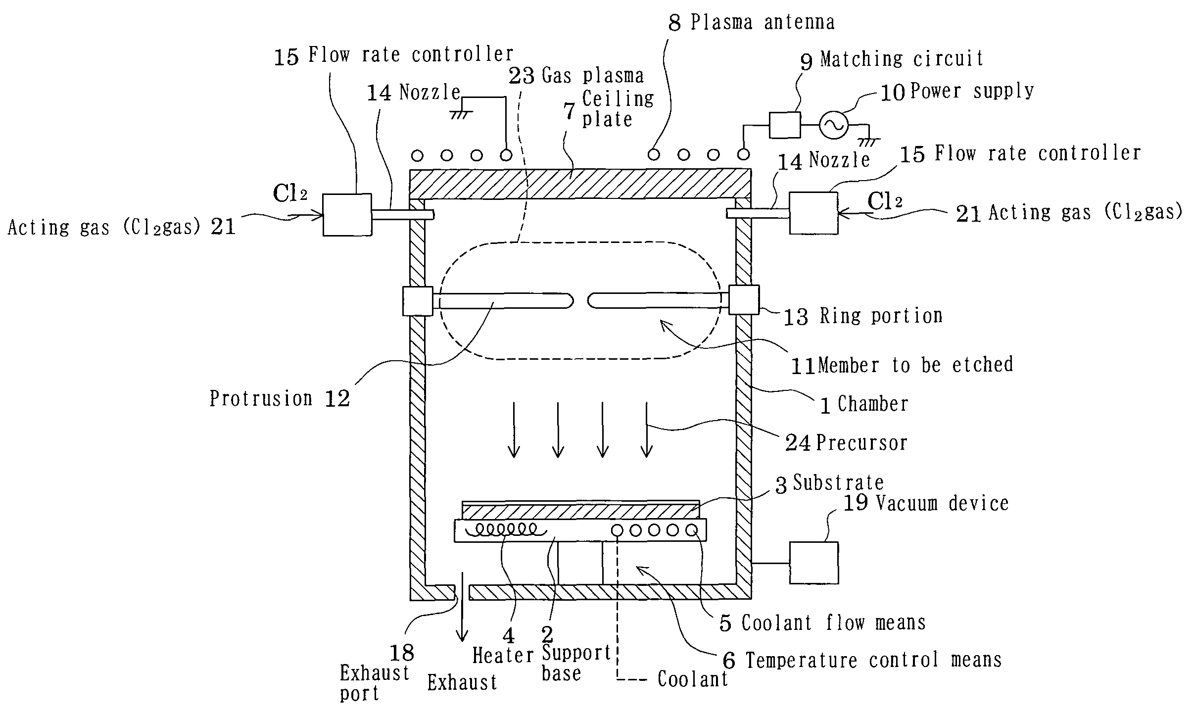
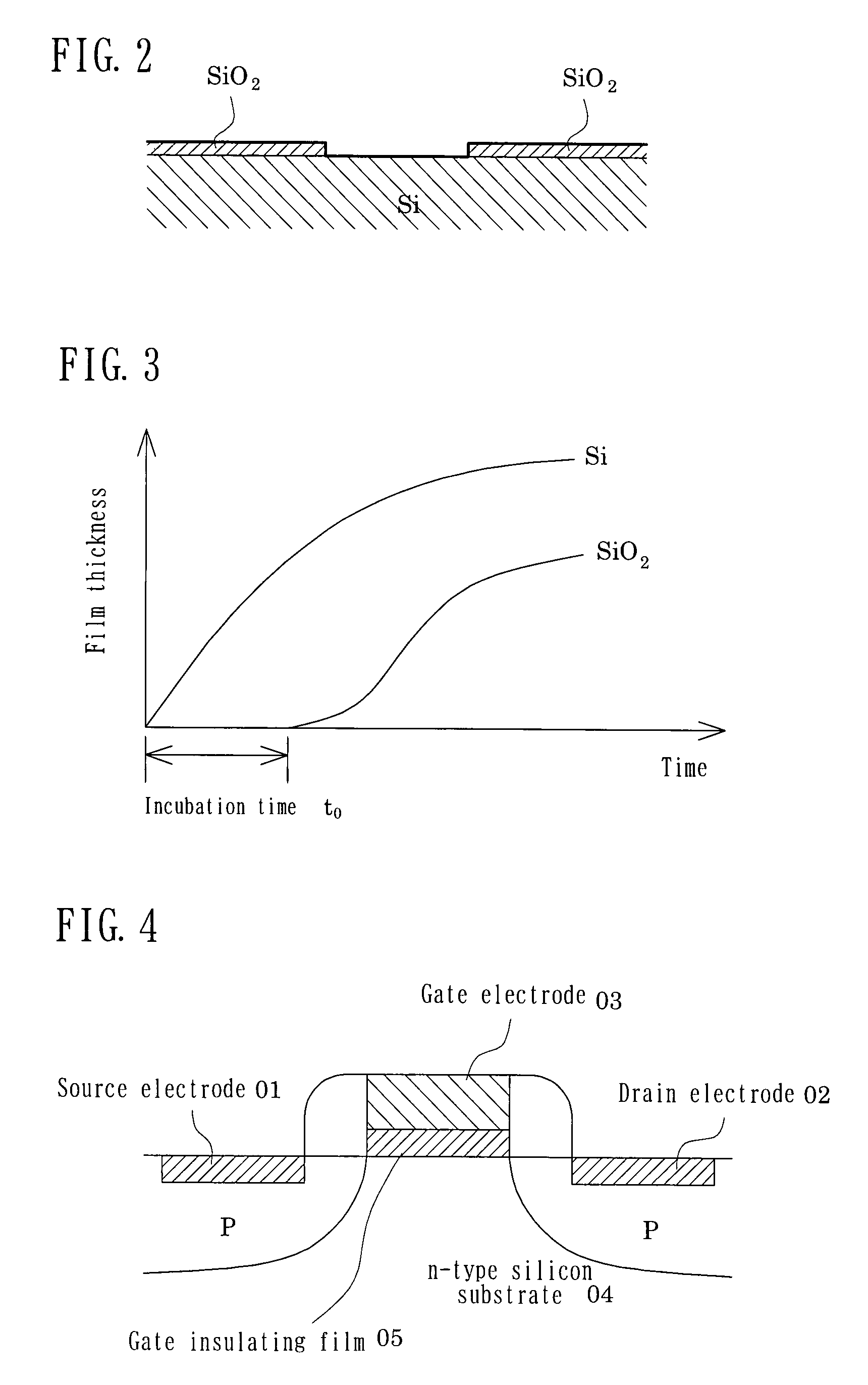
[0057]This example is an example in which NiSi is produced as the source electrode 01 and the drain electrode 02 of the MOS transistor shown in FIG. 4. The substrate 3 in this case is in a state in which a SiO2 film is formed on a Si substrate, and the SiO2 film at sites where the source electrode 01 and the drain electrode 02 are to be formed is removed, with the Si interface being exposed at these sites. The substrate 3 of such a configuration is placed on the support base 2 within the chamber 1 of the apparatus shown in FIG. 1. At this time, the member 11 to be etched is formed of Ni.

[0058]Using such an apparatus, the Cl2 gas 21 is supplied to the interior of the chamber 1 through the nozzles 14, and a high frequency electromagnetic wave is thrown by the plasma antenna 8 into the chamber 1. By so doing, the Cl2 gas 21 is ionized to generate the Cl2 gas plasma 23 and generate Cl radicals. As a result, the following reactions are caused within the chamber 1, whereby the source elec...

second example

[0068]This example is an example in which the gate electrode 03 of the MOS transistor shown in FIG. 4 is formed. The substrate 3 in this case is in a state in which a Si interface, such as polysilicon for formation of the gate electrode 03, is exposed. This substrate 3 is placed on the support base 2 within the chamber 1 of the apparatus shown in FIG. 1. At this time, the member 11 to be etched is formed of Ni.

[0069]Using such an apparatus, the Cl2 gas 21 is supplied to the interior of the chamber 1 through the nozzles 14, and a high frequency electromagnetic wave is thrown by the plasma antenna 8 into the chamber 1. By so doing, the Cl2 gas 21 is ionized to generate the Cl2 gas plasma 23 and generate Cl radicals. As a result, the following reactions are caused within the chamber 1, whereby the gate electrode 03 comprising a NiSi film at the Si interface can be formed.

third example

[0070]This example is an example in which the gate stack of the MOS transistor shown in FIG. 4 is formed. The SiO2 film which is the gate insulating film 05 is formed on the n-type silicon substrate 04 as the substrate 3 in this case. A Ni film is formed on the gate insulating film 05 by the same method as in the above examples. By this measure, a part of the Si component of SiO2 reacts with Ni to form a NiSi film as the gate electrode 03.


PUM

PropertyMeasurementUnit
temperatureaaaaaaaaaa

Abstract

A process for producing a silicon compound can minimize the number of steps and can form a desired compound in a low-temperature environment. The process comprises: allowing a radical of a halogen gas to act on a member 11 to be etched, which is disposed within a chamber 1 and is formed of a material containing an element capable of forming a compound with Si, while keeping the member 11 at a relatively high temperature, to form a gas of a precursor 24, which is a compound of the material and the halogen; holding a substrate 3 accommodated within the chamber 1 at a relatively low temperature, with the Si interface of the substrate 3 being exposed, to adsorb the precursor 24 onto the Si interface of the substrate 3; and then allowing the radical of the halogen gas to act on the precursor 24 adsorbed onto the Si interface to reduce the precursor 24, thereby producing a compound of the material and Si.

Description

TECHNICAL FIELD[0001]This invention relates to a process for producing a silicon compound, more particularly, that useful when applied in forming a metal silicide for use, for example, in an electrode of an MOS transistor.BACKGROUND ART[0002]FIG. 4 is an explanation drawing showing an MOS transistor conceptually. As shown in this drawing, the MOS transistor has two p-regions formed on an n-type silicon substrate 04, a source electrode 01 and a drain electrode 02 formed in the respective p-regions, and a gate electrode 03 formed on the n-type silicon substrate 04 via a gate insulating film 05 which is a SiO2 film. Such an MOS transistor having a NiSi film formed as the source electrode 01, the drain electrode 02 or the gate electrode 03 is produced.[0003]In this case, heat treatment at 450° C. is necessary for silicidization of Ni. However, Ni which has been deposited for the formation of NiSi, or an impurity with which a semiconductor has been doped, may be diffused to cause defects...

Claims


Application Information

Patent Timeline
Patent Type & Authority Patents(United States)
IPC IPC(8): H01L21/302H01L21/461
CPCC01B33/06C23C16/325C23C16/42C23C16/4488H01L21/2807H01L21/28097H01L21/28518H01L31/032Y02E10/50H01L21/18H01L21/24H01L31/04
Inventor OOBA, YOSHIYUKISAKAMOTO, HITOSHI
Owner CANON ANELVA CORP
Why Eureka
Try Eureka