
Ferroelectric memory and method for manufacturing same

a technology of ferroelectric memory and manufacturing method, which is applied in the field of ferroelectric memory and manufacturing same, can solve the problems of deterioration of characteristics, affecting the quality of the product, and requiring a much greater amount of etching in the prior art, so as to achieve the effect of fr

Inactive Publication Date: 2005-05-31
ROHM CO LTD
View PDF15 Cites 0 Cited by
  • Summary
  • Abstract
  • Description
  • Claims
  • Application Information

AI Technical Summary

Benefits of technology

[0006]It is therefore a primary object of the present invention to provide a ferroelectric memory having a ferroelectric characteristic that is free from deterioration, and a method for manufacturing same.
[0009]A hollow is formed in a top surface of an insulation film, and a lower electrode is formed in the hollow by a process including a spin coating method (e.g. sol-gel method). In a spin-application process, a precursor solution is dripped on the surface of the insulation film and splashed away by a centrifugal force. Consequently, the conductive film being formed has a thickness increased in a hollow portion that the precursor solution is ready to collect, i.e. a portion to be formed into a lower electrode, and decreased in other portion than the hollow. Accordingly, when etching the conductive film to form a lower electrode, it is satisfactory to etch only the portion other than the hollow, i.e. the thickness decreased portion of the conductive film, enabling etching in a brief time. However, where leaving the thinned portion of the conductive film for an interconnection, no etching is required. Also, if a first electrode portion is formed in a corner of the hollow by a process including a spin coating method and further a second electrode portion is formed thereon by a process including a spin coating method, a resulting lower electrode is reduced in amount of a depression caused in a top surface center. Meanwhile, if a first electron portion is formed at a hollow corner by a process including a spin coating method and further a second electrode portion is formed thereon by sputtering, a resulting lower electrode is reduced in variation of crystalline orientation thereof. If a film is formed in a predetermined depth position with respect to a top surface of the insulation film to form a hollow in the insulation film by using this film as an etch stop, the hollow will have a flat bottom surface at the predetermined depth position. Further, the film blocks the water content of the insulation film from reaching the ferroelectric through the lower electrode. Furthermore, if the lower electrode in the hollow and the insulation film at their top surfaces are planarized flush with each other, there is no necessity to etch the conductive film at portions other than the hollow in the later process. If a thin film is formed on a planarized lower electrode by using a same material as the lower electrode, eliminated is surface roughening caused on the lower electrode upon planarization.
[0010]According to the invention, it is possible to shorten a time for which the dielectric is exposed to a plasma atmosphere during a dry etch process. Thus, the ferroelectric can be prevented from being deteriorated in characteristics by a plasma effect.
[0012]Further, if a film is formed in the insulation film at a predetermined depth position with respect to a top surface thereof to form a hollow by utilizing the film as an etch stop, the hollow can be made flat in its bottom surface in the predetermined depth, making possible to stably form a lower electrode. Also, this film serves to block the moisture content of the insulation film from reaching the ferroelectric, thus preventing the ferroelectric from being deteriorated in characteristics.

Problems solved by technology

Thus, the prior art has required a much greater etch amount and hence a longer etch time.
Thus, there has been a fear of causing such problems as worsening the symmetry in hysteresis and deteriorating the characteristics of coerciveness and fatigue.

Method used


Image

  • Ferroelectric memory and method for manufacturing same
  • Ferroelectric memory and method for manufacturing same
  • Ferroelectric memory and method for manufacturing same

Examples


Embodiment Construction

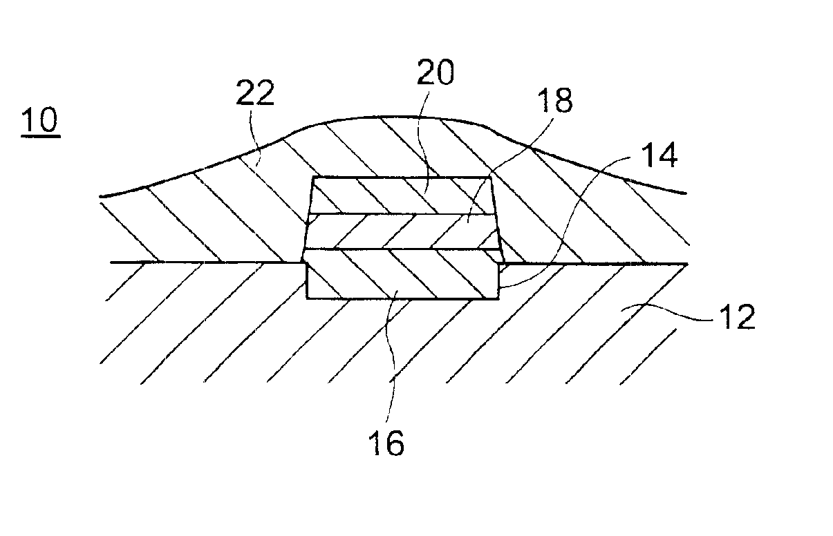
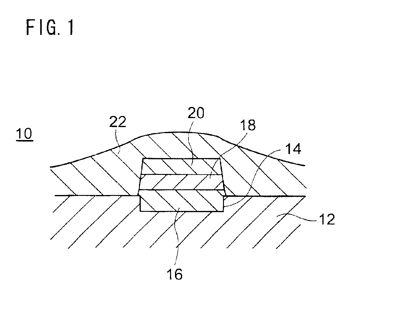
[0028]Referring to FIG. 1, there is depicted a ferroelectric memory 10 of this embodiment which includes a first insulation film 12 formed on a not-shown silicon (Si) substrate. The first insulation film 12 has a hollow 14 formed in its top surface to have a lower electrode 16 inside the hollow 14. A ferroelectric 18 and an upper electrode 20 are formed on the lower electrode 16 in this order. Further, a second insulation film 22 is formed covering these elements.

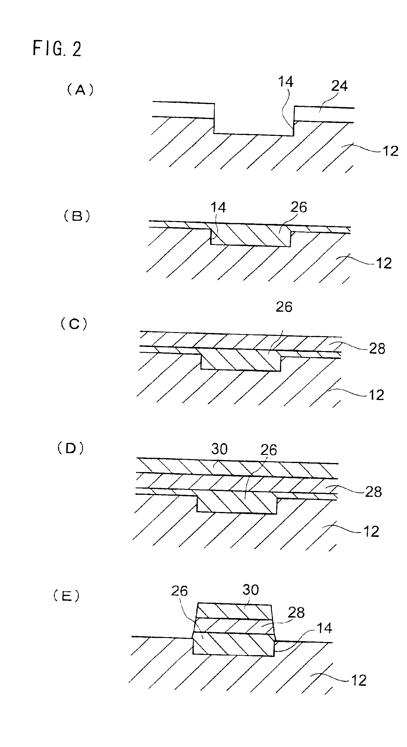
[0029]A method for manufacturing a ferroelectric memory 10 will now be explained concretely with reference to FIG. 2 and FIG. 3. First, not-shown silicon (Si) substrate is prepared, to form thereon by a CVD technique a first insulation film 12 of silicate glass containing phosphorus (PSG), silicate glass containing boron / phosphorus (BPSG) or the like. Subsequently, as shown in FIG. 2(A) the first insulation film 12 is masked by a patterned resist 24 to form a hollow 14 by an RIE (reactive ion etching) technique as anisotrop...


PUM

PropertyMeasurementUnit
thicknessaaaaaaaaaa
ferroelectricaaaaaaaaaa
conductiveaaaaaaaaaa

Abstract

Ferroelectric memory includes a hollow formed in a first insulation film. A lower electrode is formed in this hollow by sol-gel method including an application process due to a spin coat method. In this application process, a precursor solution is dripped on a surface of the first insulation film and splashed away due to centrifugal force. Due to this, a first conductive film to being formed has an increased film thickness at portion of the hollow where the precursor solution is ready to correct, or portion to be formed into a lower electrode, and a decreased film thickness at portion other than the hollow. Accordingly, it is satisfactory to etch only the hollow portion when forming a lower electrode by dry-etching the first conductive film.

Description

BACKGROUND OF THE INVENTION[0001]1. Field of the Invention[0002]This invention relates generally to a ferroelectric memory and method for manufacturing same and, more particularly, to a ferroelectric memory with a structure formed, on an insulation film, with a lower electrode, a ferroelectric and an upper electrode in this order, and a method for manufacturing such a ferroelectric memory.[0003]2. Description of the Prior Art[0004]The conventional ferroelectric memory 1 of this kind, shown in FIG. 13, includes a not-shown semiconductor substrate and a first insulation film 2 formed thereon. On the first insulation film 2, a lower electrode 3, a ferroelectric film 4 and an upper electrode 5 are formed in this order. Further, a second insulation film 6 is formed in a manner covering these films. To fabricate a ferroelectric memory 1, a conductive film 3a is formed of platinum (Pt) or the like by sputtering over the first insulation film 2 formed on the semiconductor substrate, as show...

Claims


Application Information

Patent Timeline
Patent Type & Authority Patents(United States)
IPC IPC(8): H01L21/02H01L29/51H01L29/40H10B12/00
CPCH01L28/55H01L29/516H01L28/60Y10S257/906
Inventor SAMESHIMA, KATSUMI
Owner ROHM CO LTD
Learn More