

Thin film transistor, method of manufacturing the same, organic light emitting display apparatus comprising the thin film transistor, and method of manufacturing the same
- Summary
- Abstract
- Description
- Claims
- Application Information
AI Technical Summary
Benefits of technology
Problems solved by technology
Method used
Image

Examples
Embodiment Construction
[0023]Hereinafter, the present invention will be described more fully with reference to the accompanying drawings, in which exemplary embodiments of the invention are shown.
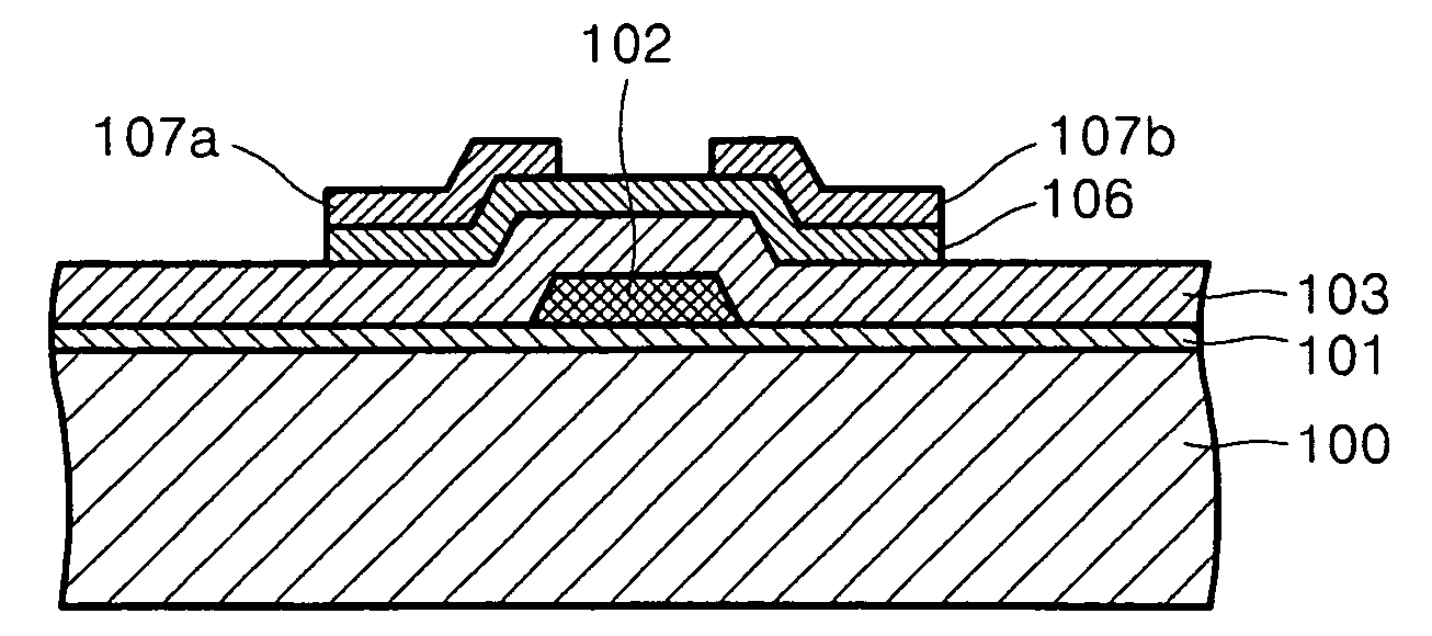
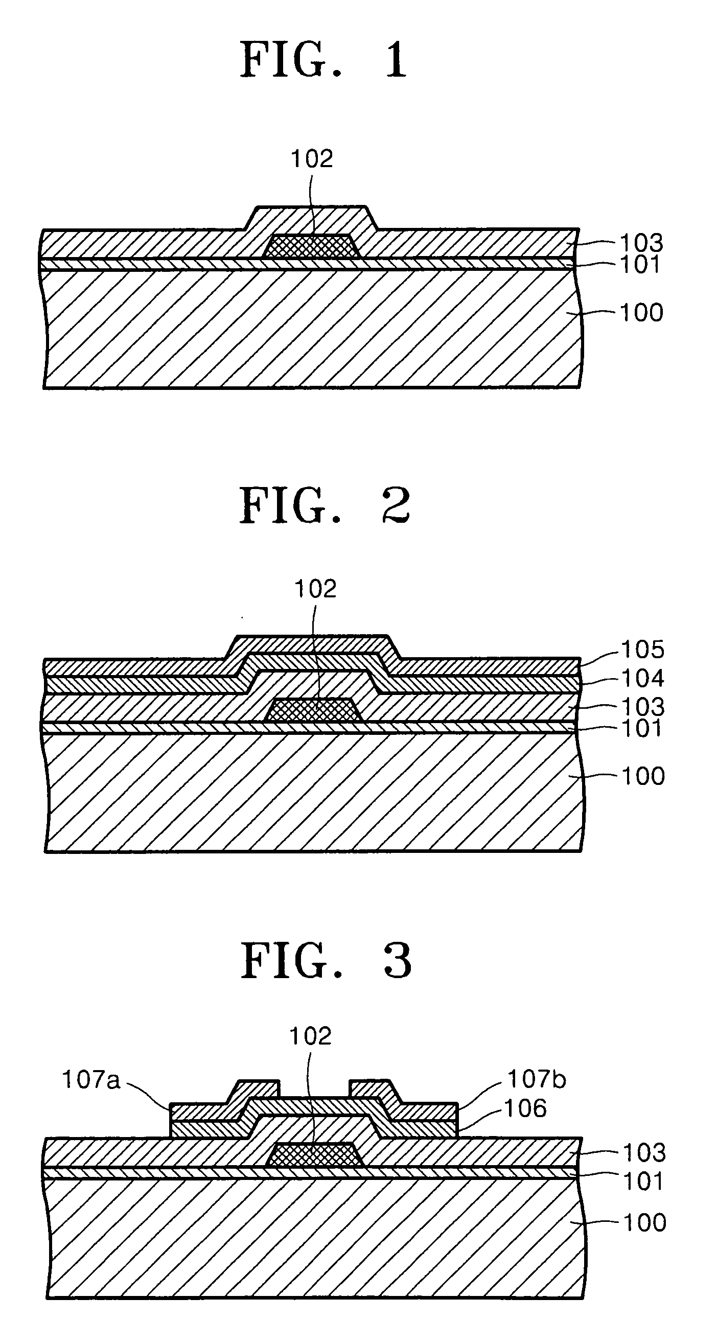
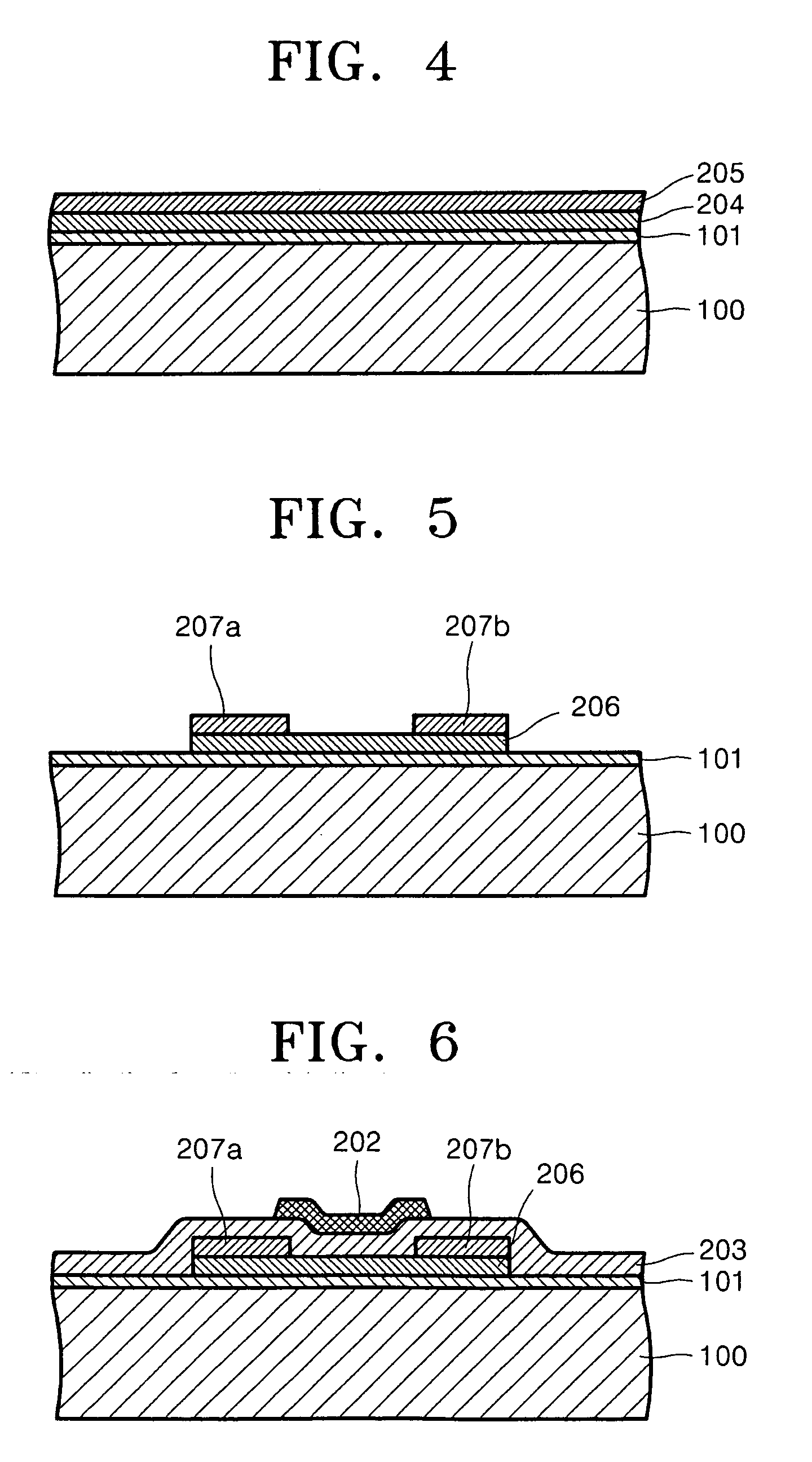
[0024]FIGS. 1 through 3 are cross-sectional views of a thin film transistor (TFT) illustrating a method of manufacturing the thin film transistor constructed as an embodiment of the present invention. The thin film transistor includes a gate electrode, an active layer, and a source and drain electrode.
[0025]The thin film transistor is formed on a substrate 100. Substrate 100 may be formed of a transparent glass material having SiO2 as a main component, however, the present invention is not limited thereto, and substrate 100 may also be formed of a transparent plastic material. The plastic substrate may be formed of an insulating organic material selected from the group consisting of polyethersulphone (PES), polyacrylate (PAR), polyetherimide (PEI), polyethyelenen napthalate (PEN), polyethyeleneterepthalate (PET),...
PUM
 Abstract
Description
Claims
Application Information