

Method of removing MEMS devices from a handle substrate
a technology of mems devices and handle substrates, which is applied in the direction of lamination, electrical equipment, lamination, etc., can solve the problems of uv light diffracting, hot air heating of adhesives, and a main rate limit step of the overall process, and achieves the effect of reducing the amount of uv light, and reducing the rate of adhesive heat dissipation
- Summary
- Abstract
- Description
- Claims
- Application Information
AI Technical Summary
Benefits of technology
Problems solved by technology
Method used
Image

Examples
Embodiment Construction
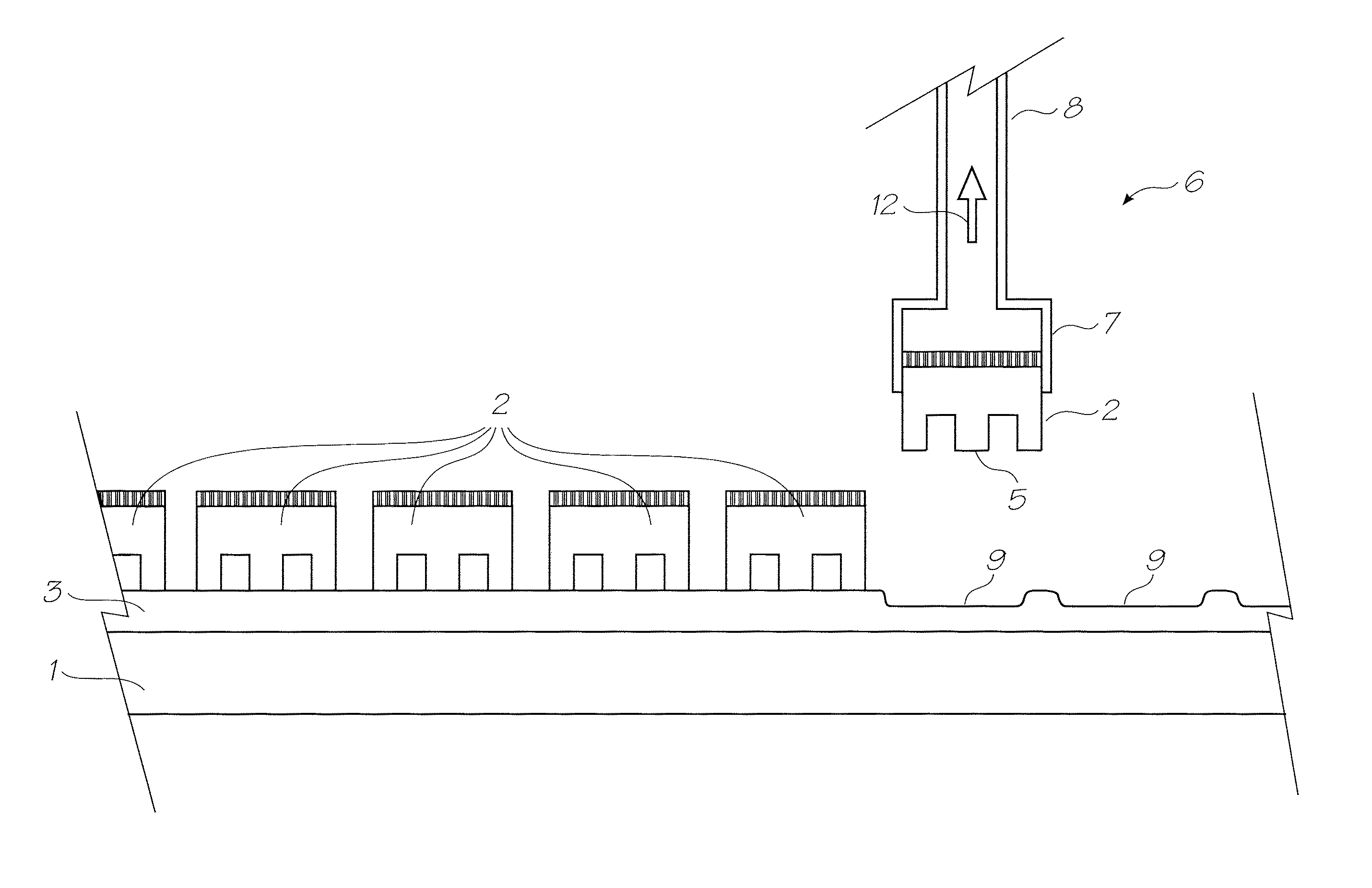
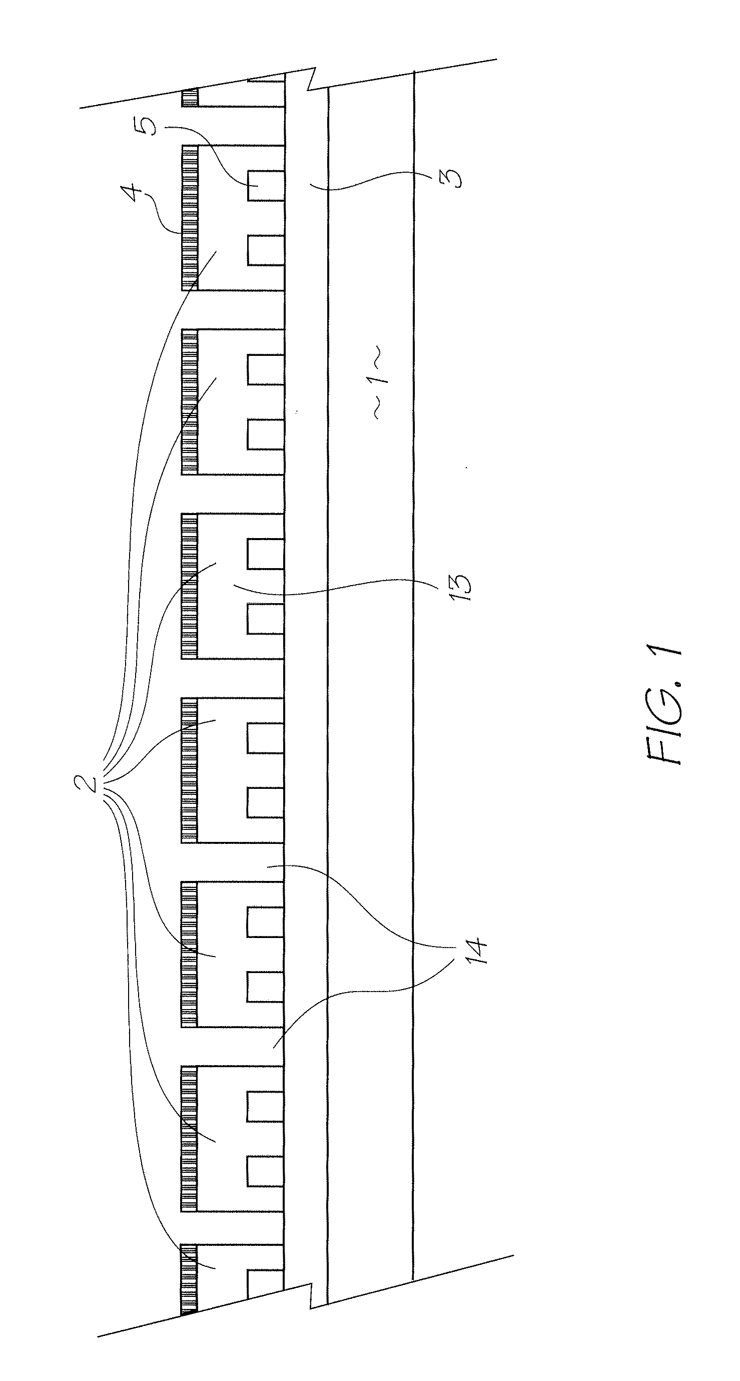
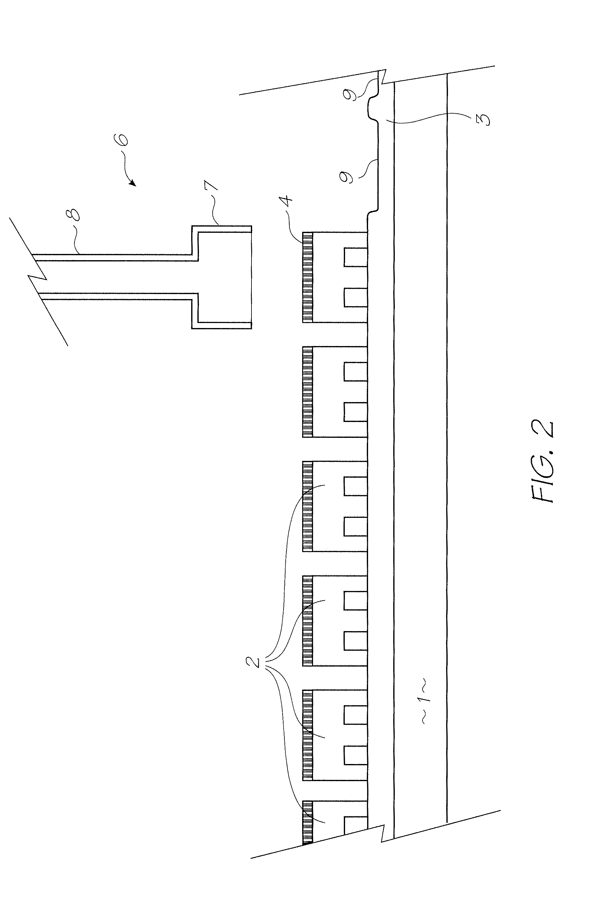
[0038]FIG. 1 shows the MEMS devices 2 bonded to the glass handle 1 by a layer of thermal release adhesive 3. The process of bonding a silicon wafer of connected dies onto a handle and subsequently dicing them into separate dies is described in the above referenced U.S. Pat. No. 6,982,184 “METHOD OF FABRICATING MEMS DEVICES ON A SILICON WAFER”. Also previously discussed, the thermal release adhesive 3 may be in the form of a film or tape which is a laminate with a thermal release adhesive layer in contact with the MEMS devices. Revalpha, V80 or W90V all made by Nitto Denko are typical of these types of release tapes. The MEMS devices 2 are shown after being diced into separate dies. As explained in the Background section, the dice streets 14 between each MEMS device 2 are formed by deep etches from the back side 5 of the silicon wafer 13. The back side 5 may also have other features etched into it such as ink feed channels. On the front side of the silicon wafer 13 are the MEMS struc...
PUM
| Property | Measurement | Unit |
|---|---|---|
| Temperature | aaaaa | aaaaa |
| Temperature | aaaaa | aaaaa |
| Temperature | aaaaa | aaaaa |
Abstract
Description
Claims
Application Information