Detector Having A Thin Film Of Boron Nitride (BN) Such As Cubic BN And Method, Systems And Array Utilizing Same

a technology of boron nitride and detector, which is applied in the field of detectors having a thin film of boron nitride (bn), can solve the problems of difficult observation of neutrons, difficult neutron interaction, and difficulty in achieving efficient neutron detectors

Inactive Publication Date: 2008-12-04
RGT UNIV OF MICHIGAN
View PDF20 Cites 16 Cited by
  • Summary
  • Abstract
  • Description
  • Claims
  • Application Information

AI Technical Summary

Benefits of technology

[0043]Still further in carrying out the above object and other objects of the present invention, an imaging system for imaging neutron emissions is provided. The system includes an array of solid-state detectors. Each of the detectors has a thin film of BN to receive the neutron emissions. The concentration of boron is sufficient to generate neutron-induced ionizing radiation in response to neutron absorptions and for generating an electrical signal in response to the neutron absorptions. The system also includes an array of sheets of high-density material for separating adjacent solid-state detectors.

Problems solved by technology

The technical difficulty in achieving an efficient neutron detector comes from the way neutrons interact with matter.
Neutrons are relatively difficult to observe because, in general, they only interact with select nuclei and the interaction probability is small.
An immediate consequence is that the size of the detector increases accordingly, this being the reason why state of the art neutron detectors are currently large and cumbersome.
Since h-BN is highly insulating, the collection of the charge carriers produced by the neutron capture event has a very low efficiency.
A drawback comes from the fact that the neutrons are absorbed outside the devices, again reducing the overall efficiency.
Another disadvantage is the charge reabsorption outside the detection element (the diode).

Method used


Image

  • Detector Having A Thin Film Of Boron Nitride (BN) Such As Cubic BN And Method, Systems And Array Utilizing Same
  • Detector Having A Thin Film Of Boron Nitride (BN) Such As Cubic BN And Method, Systems And Array Utilizing Same
  • Detector Having A Thin Film Of Boron Nitride (BN) Such As Cubic BN And Method, Systems And Array Utilizing Same

Examples


Embodiment Construction

)

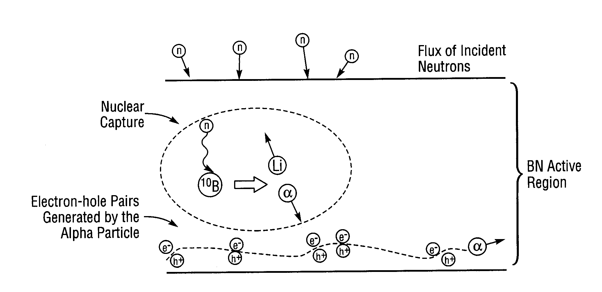
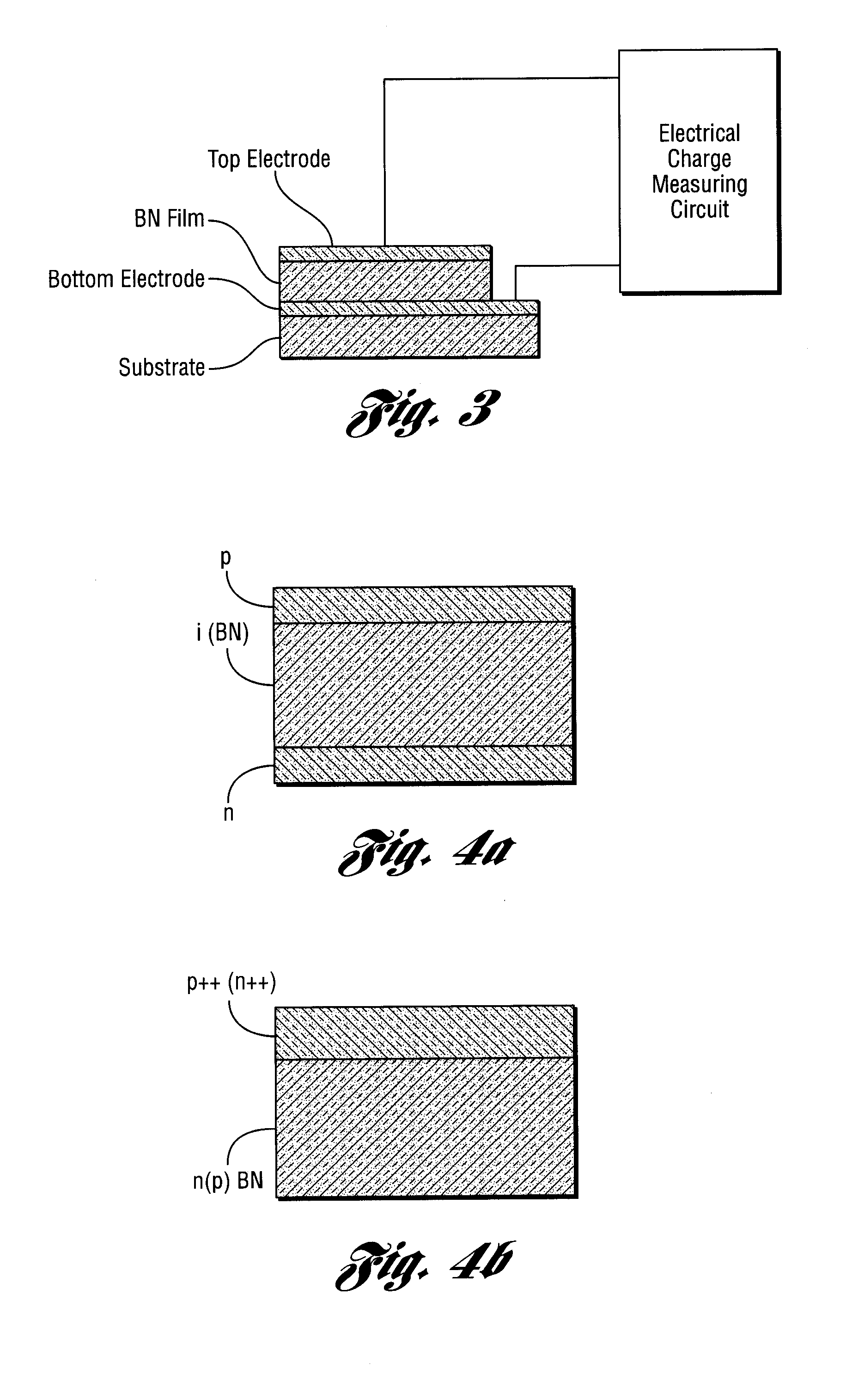
[0050]Briefly, a detector having a thin film of cubic BN and a method, systems and an array utilizing same are provided. The detector may be a diode detector based on thin semiconductor films of the cubic form of boron nitride. The advantage of the cubic form of BN for this type of application lies in the synergy between the semiconductor behavior and the ability to capture neutrons [1, 3, 4, 5]. Since it is a semiconductor, it can be doped both p- and − type. This feature enables the implementation of a p-i-n device (i.e., FIG. 4a), a deep depletion p-n device (i.e., FIG. 4b) and a Schottky device (not shown). Such a solid-state detector device is based on planar arrangements such as p-n, p-i-n or Schottky, where, for every type of structure, at least one of the p-, − and i-layers refer to thin films of cubic BN. However, it is to be understood that there are a variety of diode architectures that are possible with the detector of the present invention.

[0051]The term “thin film” re...


PUM


Abstract

A detector having a thin film of boron nitride (BN) such as cubic BN, and method, system and array utilizing same are provided. Solid-state p-i-n, deep depletion p-n and Schottky diode detector devices based on a thin film of semiconducting cubic BN are provided. Miniaturized solid-state detectors based on cubic boron nitride have a broad range of applications, both civilian and military.

Description

CROSS-REFERENCE TO RELATED APPLICATION[0001]This application claims the benefit of U.S. Provisional Application Ser. No. 60 / 933,025 filed Jun. 4, 2007.STATEMENT REGARDING FEDERALLY SPONSORED RESEARCH OR DEVELOPMENT[0002]This invention was made with government support under N66001-03-D-0042 awarded by NAVY / SPAWAR. The government has certain rights in the invention.BACKGROUND OF THE INVENTION[0003]1. Field of the Invention[0004]This invention relates to detectors having a thin film of boron nitride (BN) such as cubic BN and methods, systems and arrays utilizing same.[0005]2. Background Art[0006]The following references are related to the invention and may be referenced herein:[0007]1. G. F. Knoll, “Radiation detection and measurement,” 3 edition, Wiley, 2000.[0008]2. See, Broad Area Announcement on Nuclear Materials and Security, Department of Homeland Security, Federal Register, 2006.[0009]3. D. Litvinov and Roy Clarke, “Reduced bias growth of pure-phase cubic boron nitride,” Appl. P...

Claims


Application Information

Patent Timeline
Patent Type & Authority Applications(United States)
IPC IPC(8): G01T3/08
CPCG01T3/08
Inventor CLARKE, ROYCIONCA, CODRIN N.
Owner RGT UNIV OF MICHIGAN
Why Eureka
Try Eureka