Solid state back-illuminated photon sensor

a photon sensor and solid-state technology, applied in semiconductor/solid-state device manufacturing, electrical equipment, semiconductor devices, etc., can solve the problems of poor ultraviolet-visible, 300-750 nm) image resolution, backside illumination produces problems that are not present, etc., to minimize etaloning spanning the nir spectrum

Active Publication Date: 2011-07-21
TELEDYNE DIGITAL IMAGING US INC
View PDF7 Cites 17 Cited by
  • Summary
  • Abstract
  • Description
  • Claims
  • Application Information

AI Technical Summary

Benefits of technology

[0013]An embodiment of the present invention address the needs described above by providing a solid state imaging sensor employing an anti-reflection structure in the form of layered dielectric refractory metal oxides and / or metal fluorides deposited via physical vapor deposition atop of the photosensitive region of the solid state imaging sensor, in such a way as to minimizing etaloning spanning the NIR spectrum while retaining high device QE over the UV-NIR spectrum.

Problems solved by technology

However, backside illumination produces problems not present in traditional front-illuminated sensors.
A back thinned sensor having too thin a Si epitaxial layer results in poor near infrared (NIR: 750-1100 nm) response while too thick a layer results in poor ultraviolet-visible (UV-VIS: 300-750 nm) image resolution via a reduction in modulation transfer function and higher dark current.
Etaloning is difficult to predict in advance of any scientific measurement and presents a problem that must be overcome when using back-illuminated imaging sensors.
This problem is further complicated for spectroscopic applications because nearly all optical spectrometers have a mechanically driven diffraction grating which allows the user to change the region of the electromagnetic spectrum in question thus changing entirely the observed modulation in detector sensitivity.
Single layer AR coatings of this type will produce approximately a ‘U’ shaped reflectivity curve and therefore can only enhance the image sensor's QE over a limited wavelength range.
However, the QE of the image sensor will suffer greatly in the UV-VIS portion of the spectrum due to increased backside surface reflectivity.
As a result, this type image sensor is only useful for a single type spectrometer or spectrophotometer having fixed spectral dispersion characteristics as defined by the image sensor's graded AR coating.

Method used


Image

  • Solid state back-illuminated photon sensor
  • Solid state back-illuminated photon sensor
  • Solid state back-illuminated photon sensor

Examples


Embodiment Construction

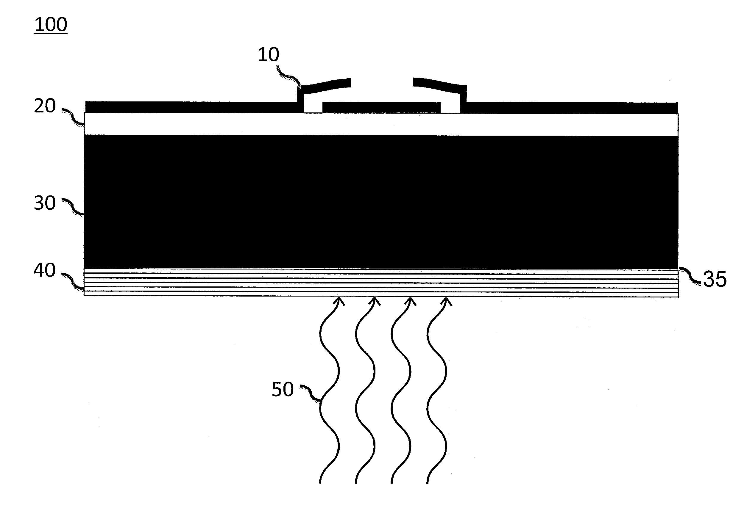
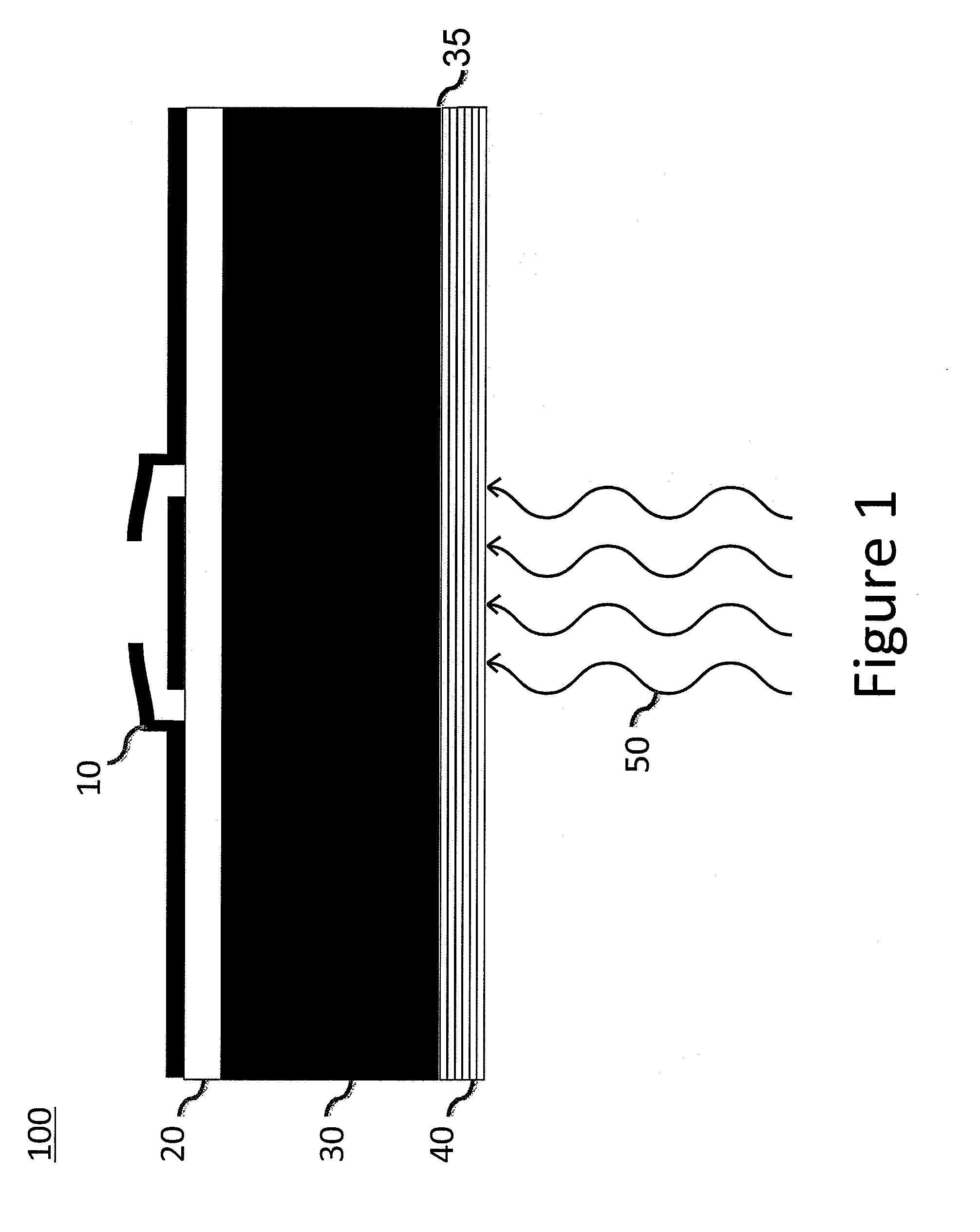
[0026]The term “substrate” herein means the photosensitive Si epitaxial layer on which light is incident, which is an intimate part of a solid state detector, which may be a charge coupled device (CCD), CMOS, or EM-CCD sensor. The term “anti-reflection structure” herein means a multi-layer thin-film coating applied to the backside surface of the substrate.

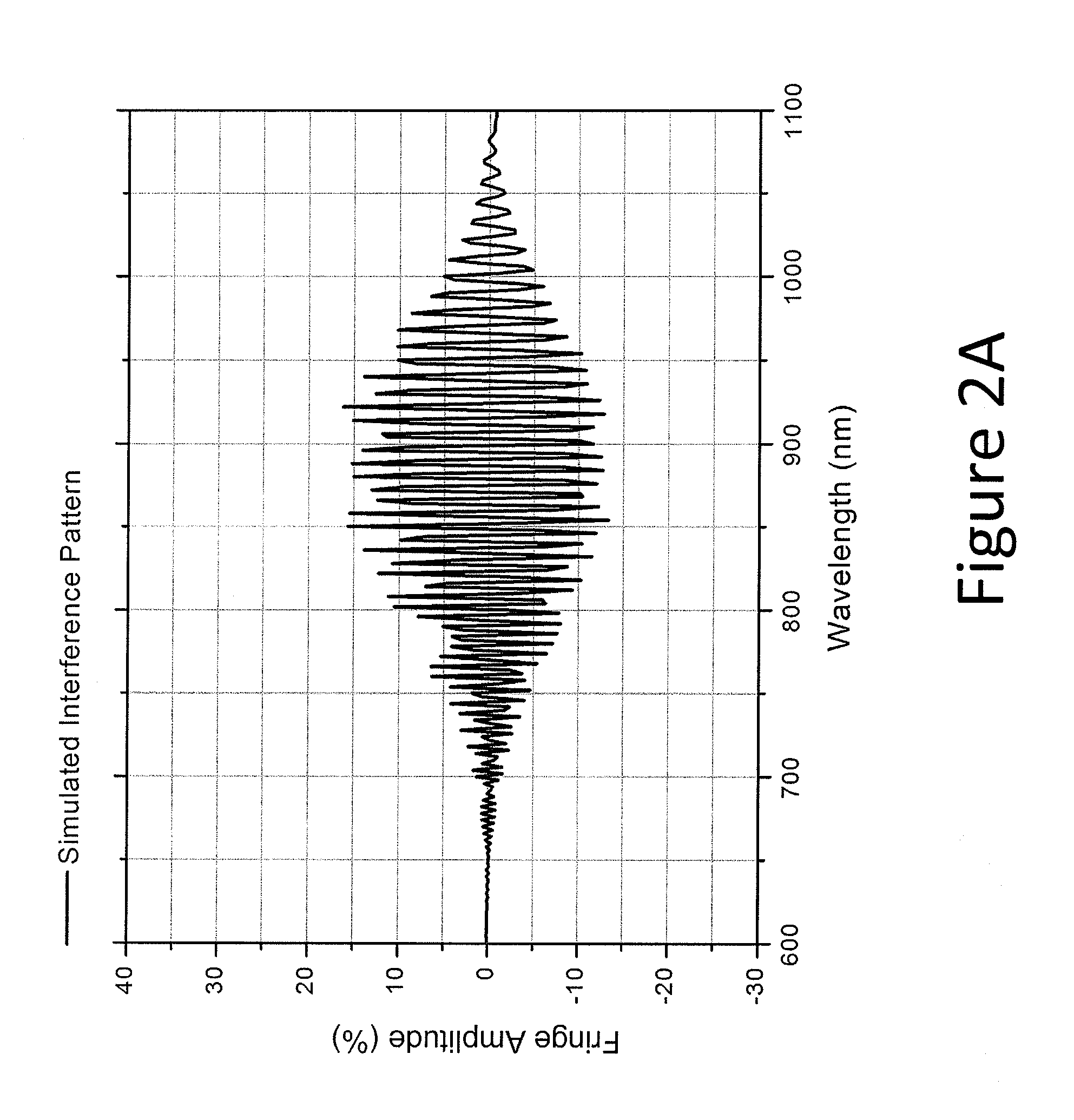
[0027]Disclosed herein is a backside-illuminated solid state imaging sensor employing an anti-reflection structure in the form of layered dielectric refractory metal oxides and / or metal fluorides applied to the backside surface of said sensor's photosensitive Si epitaxial layer. This novel image sensor provides a new class of back-illuminated solid state detectors for imaging. The layered anti-reflection structure is designed specifically reduce the occurrence of interference fringes in the NIR while maintaining a high QE over a broad range of wavelengths (300-1100 nm).

[0028]FIG. 1 schematically illustrates the inventive solid stat...


PUM


Abstract

A backside-illuminated image sensor is disclosed having improved quantum efficiency (QE) in the near infrared wavelengths (NIR: 750-1100 nm) with minimal optical interference fringes produced by multiple reflected rays within the photosensitive Si region of the sensor, which may be a charge-coupled device, a complementary metal oxide sensor or an electron-multiplication sensor. The invention comprises a fringe suppression layer applied to the backside surface of the photosensitive Si region of a detector (Si substrate) whereby the fringe suppression layer functions in concert with the Si substrate to reduce the occurrence of interference fringes in the NIR while maintaining a high QE over a broad range of wavelengths (300-1100 nm). The combination of a fringe suppression layer applied to a Si substrate provides a new class of back illuminated solid state detectors for imaging.

Description

CROSS-REFERENCE TO RELATED APPLICATIONS[0001]This utility application claims the benefit under 35 U.S.C. §119(e) of Provisional Application Ser. No. 61 / 297,076 filed on Jan. 21, 2010 and entitled Solid State Back-Illuminated Photon Sensor. The entire disclosure of this application is incorporated by reference herein.FIELD OF THE INVENTION[0002]The invention relates to back-illuminated solid state image sensors, and particularly to methods of improving the quantum efficiency (QE) in the ultraviolet to near infrared spectrum (UV-NIR: 300-1100 nm) while minimizing interference fringes produced by internally reflected rays in the photosensitive region of the image sensor in the near infrared spectrum NIR: (750-1100 nm).BACKGROUND OF THE INVENTION[0003]Solid state image sensors produce a digital representation of a visual image by means of converting incident photons into electronic charges that are accumulated by discrete potential wells or photodiodes (pixels) setup by circuitry in the...

Claims


Application Information

Patent Timeline
Patent Type & Authority Applications(United States)
IPC IPC(8): H01L31/0232
CPCH01L27/14621H01L27/1464H01L31/02162H01L27/14685
Inventor ASHER, WILLIAM EDWARDCASE, MICHAEL ALANMCCLURE, JASON
Owner TELEDYNE DIGITAL IMAGING US INC
Why Eureka
Try Eureka