
Semiconductor device and manufacturing method thereof

a technology of mikro-onductors and transistors, which is applied in the direction of mikro-onductors, basic electric elements, electrical appliances, etc., can solve the problems of reducing the width of the fin active region, and reducing the height of the fin active region. , to achieve the effect of improving the control of the electric field at the bottom not reducing the height of the fin active region, and not reducing the width

Inactive Publication Date: 2008-12-04
ELPIDA MEMORY INC
View PDF9 Cites 76 Cited by
  • Summary
  • Abstract
  • Description
  • Claims
  • Application Information

AI Technical Summary

Benefits of technology

[0009]Another object of the present invention is to provide a semiconductor device that the cross-section of the fin active region is formed in a trapezoidal shape and control of electric field at the bottom of the fin active region is improved, and a manufacturing method thereof.
[0017]Further, because the area of the top surface of the fin active region covered by the gate electrode is small, the area that the source contact and the drain contact can be formed is ensured sufficiently. Accordingly, a margin for forming the source contact and the drain contact is ensured sufficiently, and short circuits between the gate electrode and the source and drain contacts are thus prevented.

Problems solved by technology

However, as the channel width becomes narrower, the channel resistance of the transistor is increased considerably, resulting in a decrease in drive current.
However, when the fin field effect transistor is formed, the cross-section of the fin active region may be formed in a trapezoidal shape other than a rectangular or square shape because of processing problems.
A source contact and a drain contact are thus difficult to be formed.
The height of the fin active region is reduced and desired characteristics cannot be obtained.

Method used


Image

  • Semiconductor device and manufacturing method thereof
  • Semiconductor device and manufacturing method thereof
  • Semiconductor device and manufacturing method thereof

Examples


first embodiment

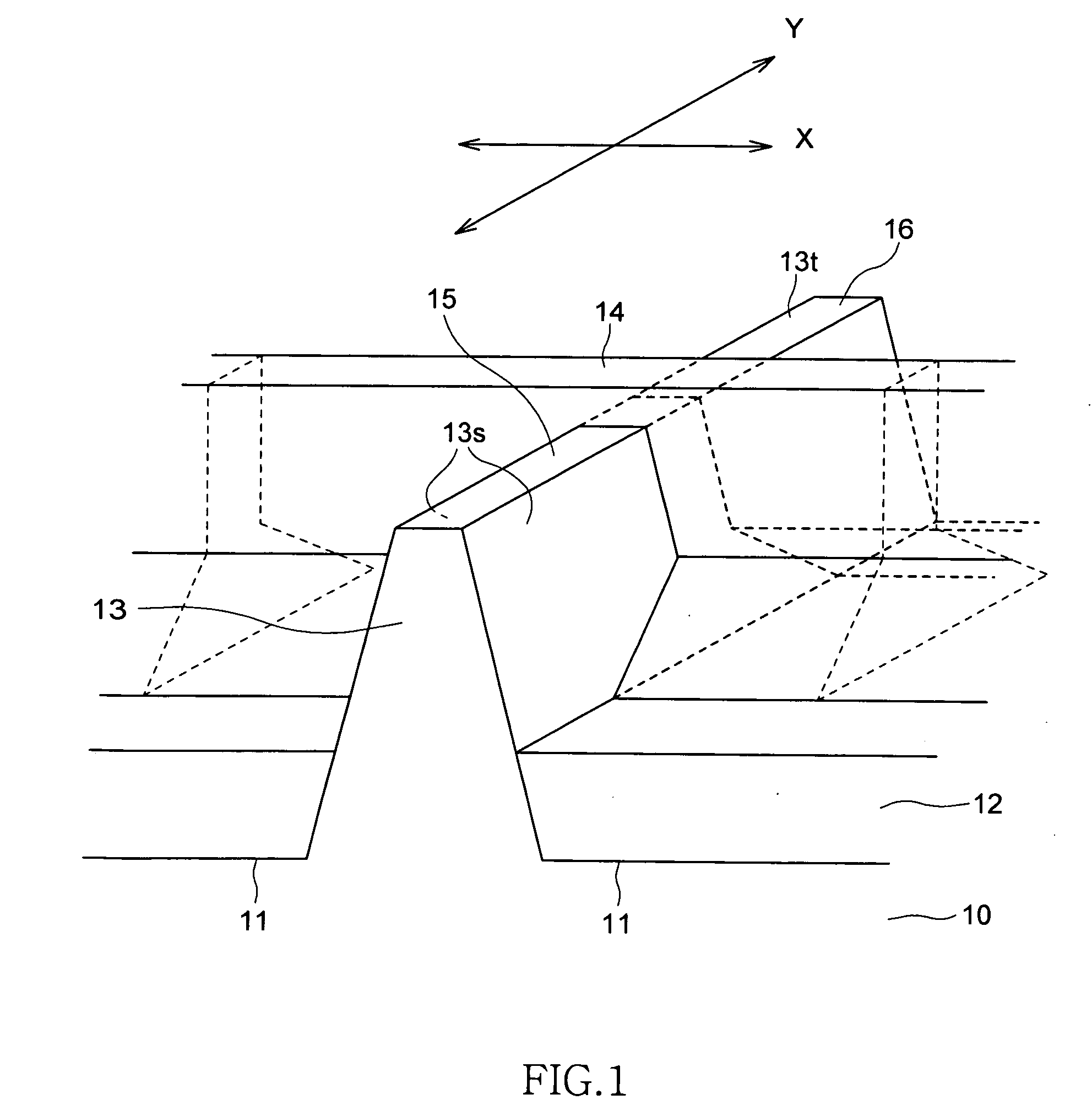
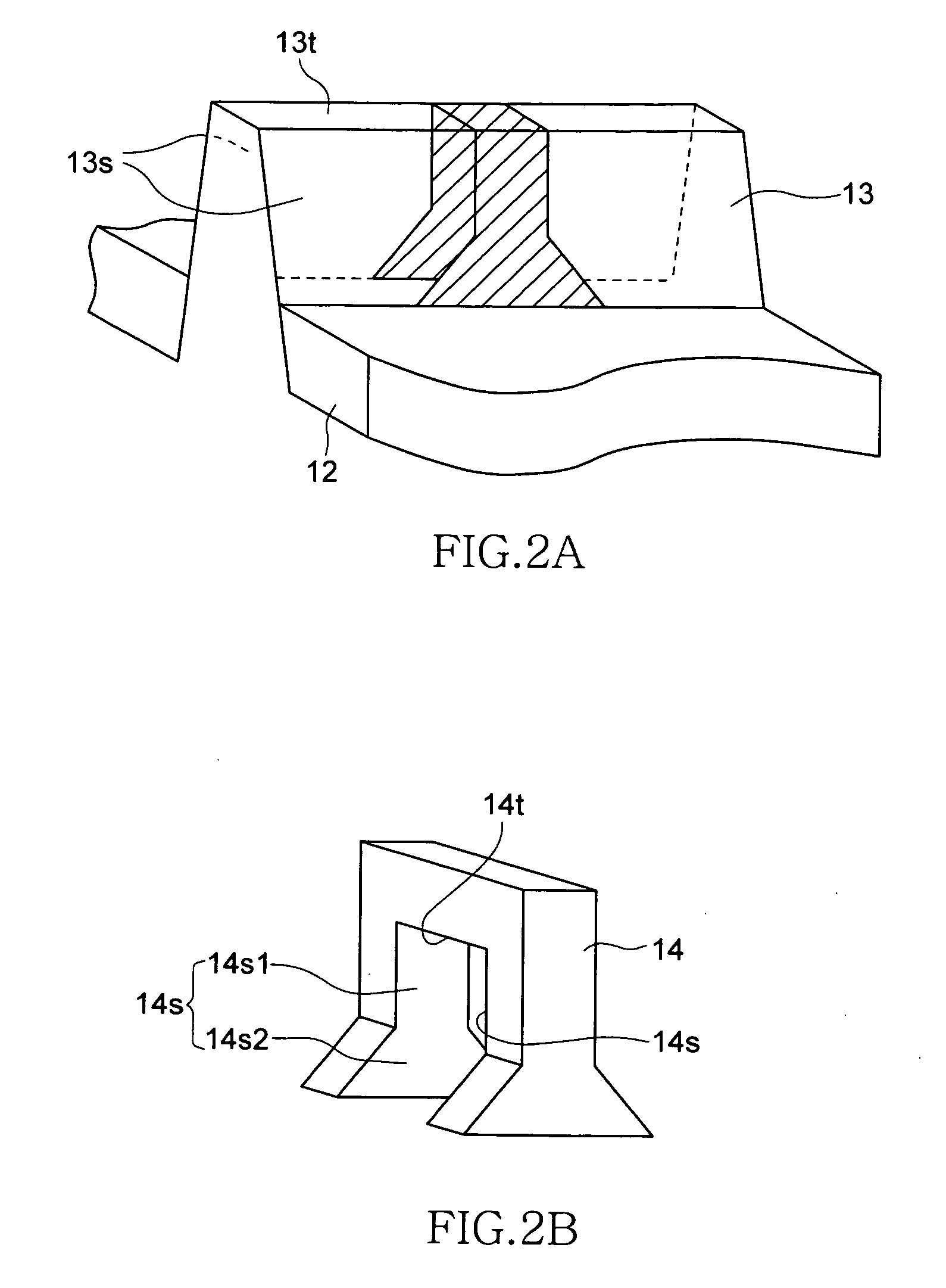
[0046]FIG. 1 is a schematic perspective view for explaining the configuration of a semiconductor device according to the present invention. FIGS. 2A and 2B are schematic exploded perspective views of the semiconductor device shown in FIG. 1.

[0047]As shown in FIG. 1, the semiconductor device according to the first embodiment has a semiconductor substrate 10, a trench 11 formed in the semiconductor substrate 10, and an STI 12 provided on the bottom of the trench 11. The STI 12 is embedded in the trench 11 from the bottom to the middle of the trench. A fin portion which is a part of the semiconductor substrate protruding upward from the STI 12 serves as a fin active region 13. The fin active region 13 extends in the Y direction shown in FIG. 1 and has a top surface 13t and two side surfaces 13s. The side surfaces 13s of the fin active region 13 are in the same planes as those of the STI 12.

[0048]As shown in FIG. 1, because the side surfaces 13s of the fin active region 13 are tapered, ...

second embodiment

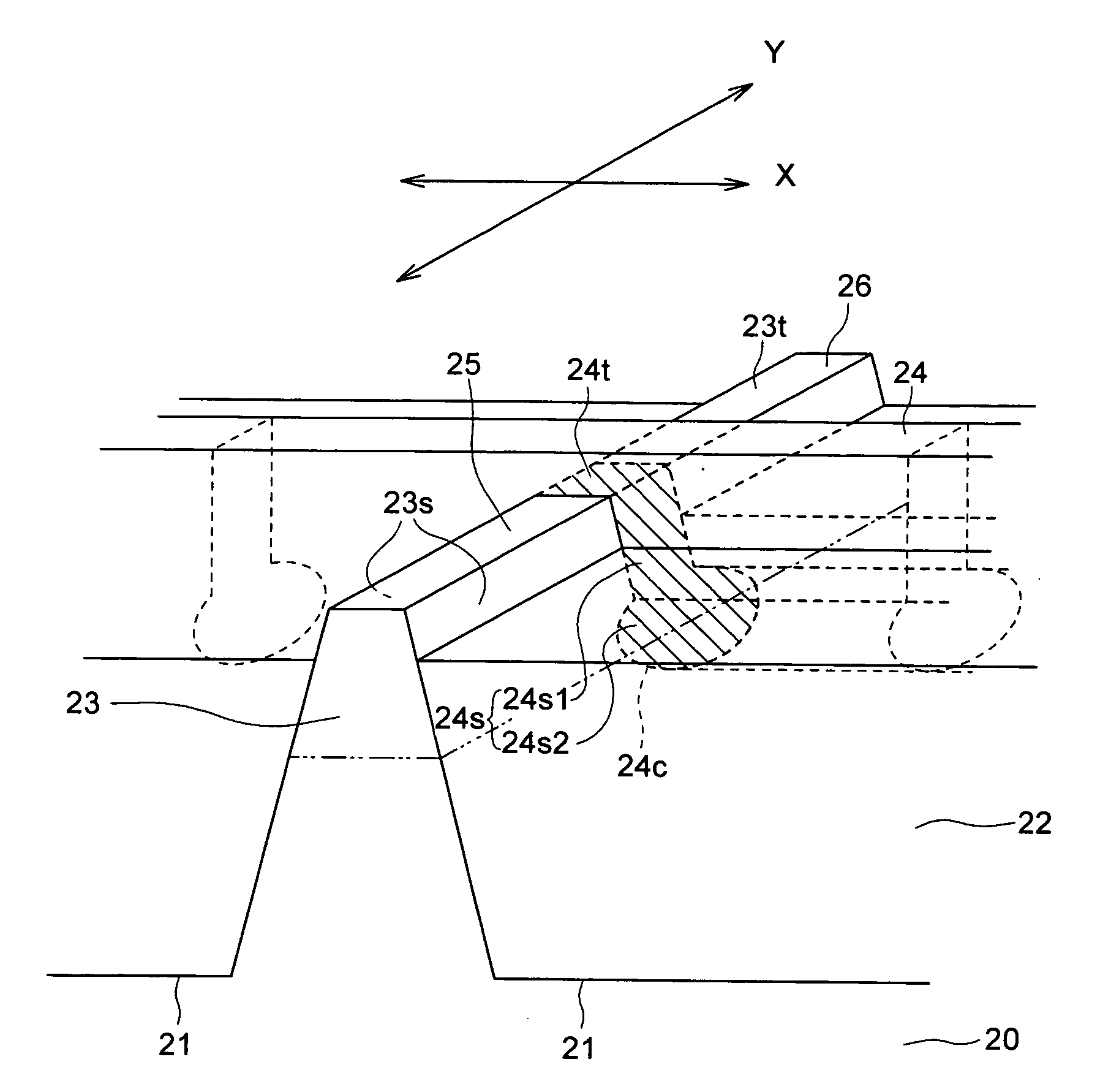
[0074]FIG. 13 is a schematic perspective view showing the configuration of a semiconductor device according to the

[0075]As shown in FIG. 13, the semiconductor device according to the second embodiment has a semiconductor substrate 20, a trench 21 formed in the semiconductor substrate 20, and an STI 22 provided at the bottom of the trench 21. The STI 22 is embedded in the trench 21 from the bottom to the middle of the trench.

[0076]Unlike the first embodiment, in the second embodiment, a part of the semiconductor substrate with a predetermined depth from the surface of the STI 22 to the two-dot chain line in FIG. 13 as well as a fin portion which is a part of the semiconductor substrate protruding from the STI 22 serves as a fin active region 23. The fin active region 23 extends in the Y direction shown in FIG. 13 and has a top surface 23t and two side surfaces 23s. The side surfaces 23s of the fin active region 23 are in the same planes as those of the STI 22. As shown in FIG. 13, as...


PUM


Abstract

A semiconductor device includes a fin active region with a tapered side surface, a gate electrode that has a side surface covering portion covering a part of the side surface of the fin active region and a top surface covering portion covering a part of a top surface of the fin active region, and a source region and drain region formed in the fin active region. In at least a part of the side surface covering portion of the gate electrode, the width is wider at its bottom than at its top. Control of electric field by the gate electrode is improved. Punch-through is thus prevented.

Description

TECHNICAL FIELD[0001]The present invention relates to a semiconductor device and a manufacturing method thereof, and, more particularly relates to a semiconductor device having a fin field effect transistor and a manufacturing method thereof.BACKGROUND OF THE INVENTION[0002]In recent years, along with miniaturization of DRAM (Dynamic Random Access Memory) cells, the gate length of a memory cell transistor needs to be shortened and the channel width needs to be made narrower. However, as the channel width becomes narrower, the channel resistance of the transistor is increased considerably, resulting in a decrease in drive current.[0003]As a technique for preventing such a problem, fin field effect transistors have attracted attention that a narrow active region is formed like a fin in a direction perpendicular to a semiconductor substrate and a gate electrode is placed around the active region (see Japanese Patent Application National Publication No. 2005-528810, Japanese Patent Appl...

Claims


Application Information

Patent Timeline
IPC IPC(8): H01L29/00H01L21/336
CPCH01L29/66621H01L29/66795H01L29/7853
Inventor MIKASA, NORIAKI
Owner ELPIDA MEMORY INC
Features
  • Generate Ideas
  • Intellectual Property
  • Life Sciences
  • Materials
  • Tech Scout
  • Unparalleled Data Quality
  • Higher Quality Content
  • 60% Fewer Hallucinations
Learn More