
Parametric testline with increased test pattern areas

a parametric testline and test pattern technology, applied in the direction of individual semiconductor device testing, semiconductor/solid-state device testing/measurement, instruments, etc., can solve the problem that the size of the test pattern area on a prior art parametric testline will become too small to accommodate certain types of duts, increase circuit complexity, and impose new demands on the existing parametric testline structure, etc. problem, to achieve the effect of improving the utilization of test line spa

Active Publication Date: 2008-12-11
TAIWAN SEMICON MFG CO LTD
View PDF4 Cites 7 Cited by
  • Summary
  • Abstract
  • Description
  • Claims
  • Application Information

AI Technical Summary

Benefits of technology

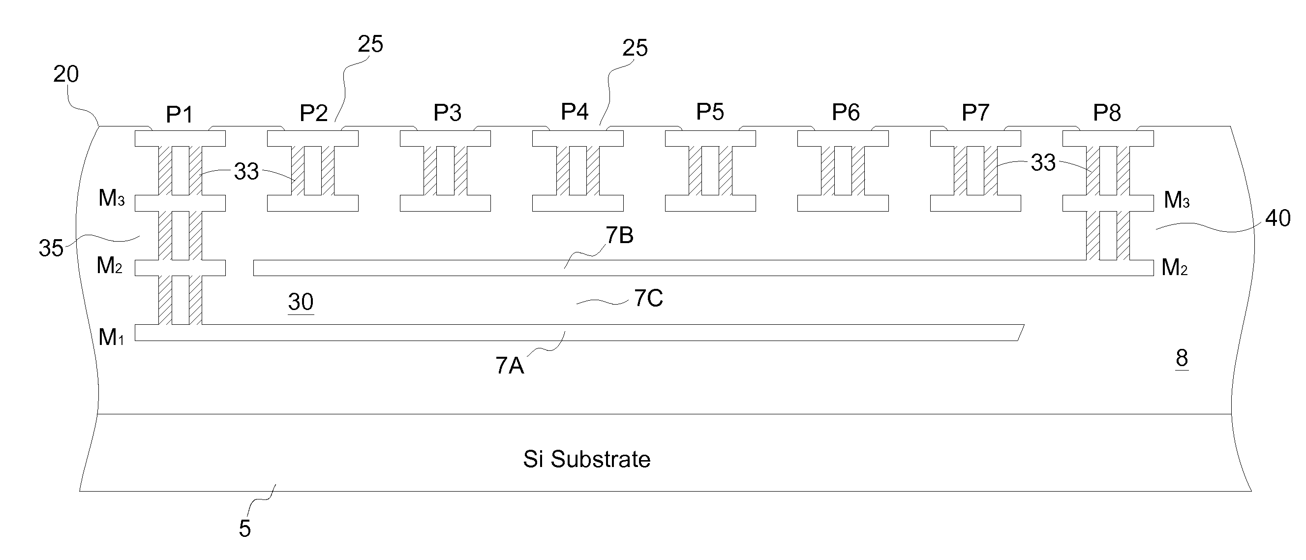
[0012]Several advantageous features are provided by preferred embodiments of the present invention. These include significant improvements on testline space utilization. The designed structure of a conventional parametric testline only allows a DUT being formed in a test pattern area between adjacent probe pads. The para metric testline structure of this invention allows large size DUTs to be formed in a space underlying a plurality of probe pads. The parametric testline structure of this invention also allows DUTs to be formed in a stacking configuration. Moreover, comparing to the square or rectangular probe pad shape and pad orientation in a prior art testline, the probe pad shapes and orientation in preferred embodiments can be altered so that a test pattern area between adjacent probe pads can be maximized to accommodate DUTs of large sizes. As a result, more DUTs and DUTs of various shape and dimensions can be formed in a shrunk testline of the current invention.

Problems solved by technology

As a result, at a certain point, the size of a test pattern area on a prior art parametric testline will become too small to accommodate certain types of DUTs.
On the other hand, the continuing scale-down of device feature sizes and increased circuit complexity in an integrated circuit has imposed new demands on the existing parametric testline structure.

Method used


Image

  • Parametric testline with increased test pattern areas
  • Parametric testline with increased test pattern areas
  • Parametric testline with increased test pattern areas

Examples


Embodiment Construction

[0023]The making and using of the presently preferred embodiments are discussed in detail below. It should be appreciated, however, that the present invention provides many applicable inventive concepts that can be embodied in a wide variety of specific contexts. The specific embodiments discussed are merely illustrative of specific ways to make and use the invention, and do not limit the scope of the invention.

[0024]The present invention will be described with respect to preferred embodiments in a specific context, namely innovative parametric testline structures for wafer acceptance testing (WAT). The preferred embodiments of the present invention include testline structures offering larger test pattern areas in order to accommodate more DUTs and DUTs with large dimensions. The invention may also be applied to benefit other activities, such as process control monitoring (PCM), yield analysis, statistical split, design-of-experiment (DOE), and design-for-manufacturability (DFM), an...


PUM


Abstract

An integrated circuit parametric testline providing increased test pattern areas is disclosed. The testline comprises a dielectric layer over a substrate, a plurality of probe pads over the dielectric layer, and a first device under test (DUT) formed in the testline in a space underlying the probe pads. The testline may also include a second DUT, which is formed in a space underlying the probe pads overlying the first DUT in an overlaying configuration. The testline may further include a polygon shaped probe pad structure providing an increased test pattern area between adjacent probe pads.

Description

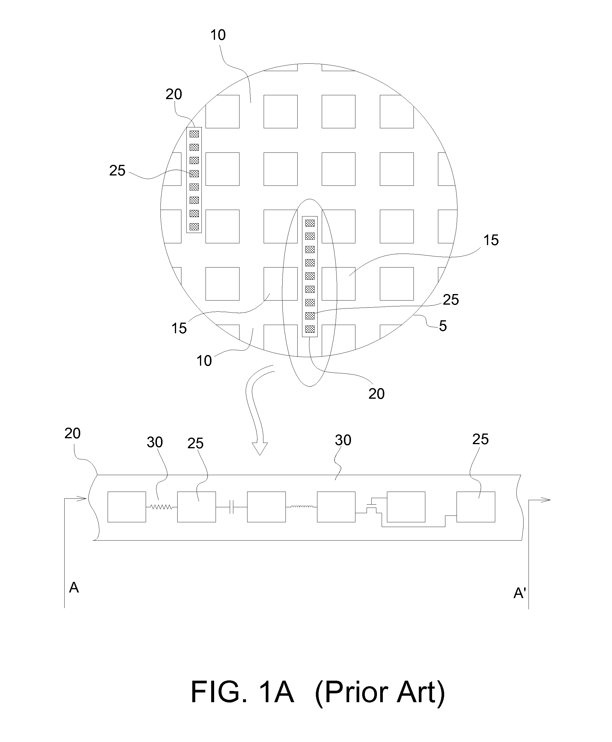
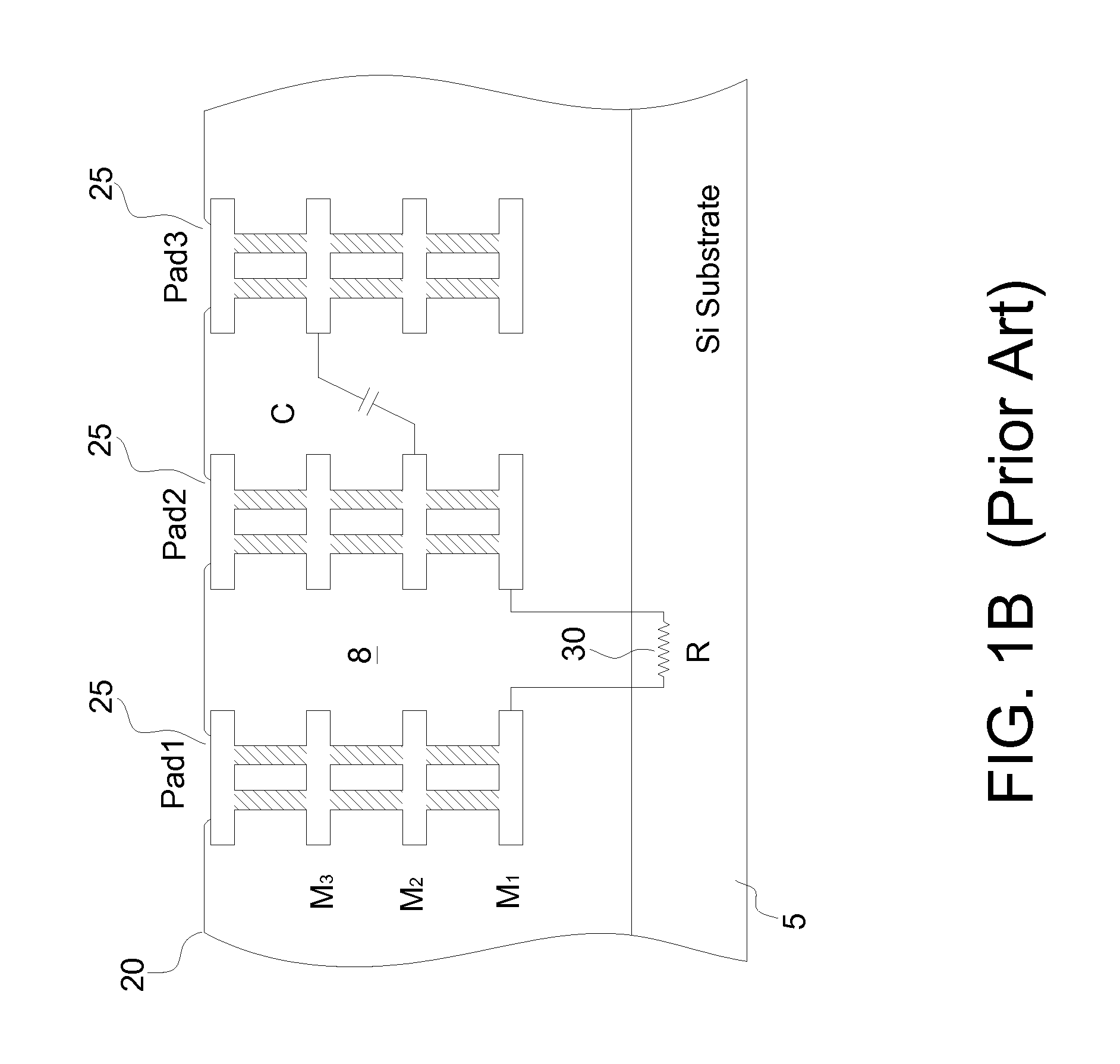
TECHNICAL FIELD[0001]The present invention relates generally to the testing of integrated circuits, and more particularly to the structure of parametric testline on an integrated circuit wafer substrate for wafer acceptance testing (WAT), process control monitoring (PCM) and other R&D testing needs.BACKGROUND[0002]In integrated circuit (IC) manufacturing, a semiconductor wafer typically contains a plurality of testlines in the scribe line area between adjacent wafer dies. Each testline includes a number of devices under test (DUTs), which are structures similar to those that are normally used to form the integrated circuit products in the wafer die area. DUTs are usually formed in the test pattern areas between adjacent probe pads on a testline at the same time as the functional circuitry using the same process steps. Probe pads are usually flat, square metal surfaces on a testline through which test stimuli can be applied to corresponding DUTs. Parametric test results on DUTs are u...

Claims


Application Information

Patent Timeline
Patent Type & Authority Applications(United States)
IPC IPC(8): G01R31/26
CPCG01R31/2884H01L2924/0002H01L22/34H01L2924/00
Inventor CHEN, HSIEN-WEIHSU, SHIH-HSUNTSAI, HAO-YIJENG, SHIN-PUU
Owner TAIWAN SEMICON MFG CO LTD
Learn More