High accuracy and universal on-chip switch matrix testline

a switch matrix and high accuracy technology, applied in the field of integrated circuit testing, can solve the problems of imposing new challenges on the existing parametric testline structure and test methodology, unable to support a limited number of test devices, and unable to meet the requirements of the testline, so as to improve the utilization of testline space and increase the flexibility of circuit design

Active Publication Date: 2008-10-02
TAIWAN SEMICON MFG CO LTD
View PDF17 Cites 18 Cited by
  • Summary
  • Abstract
  • Description
  • Claims
  • Application Information

AI Technical Summary

Benefits of technology

[0013]Advantageous features provided by preferred embodiments of the present invention include, but not limited to, improvement on testline space utilization and increased flexibility in circuit design.

Problems solved by technology

With the continuing scale-down of IC device feature sizes, integrated circuit device density and functional complexity are continuously increasing.
This trend imposes new challenges on the existing parametric testline structure and test methodologies.
One of these challenges is that the testlines of advanced technology devices must include a tremendous amount of test structures to meet the testing needs for advanced semiconductor devices and complex integrated circuits.
However, the current testline structure can only support a limited number of test devices, as known to people skilled in the art.
Another challenge is that the parametric test results on existing testline devices are gradually losing their correlation with real integrated circuit performance, as technology advances.
In current practice, these customized devices are not presented and tested on a conventional testline due to the limited available spaces for test devices.
Another challenge is the need to design-for-manufacturability (DFM) in advanced technology.
In current practice, library and test structure designers focus more on electrical characteristics than on layout styles due to their lack of visibility on the impact of layout styles on device manufacturing yield.
Due to the limitation of available test device spaces on a conventional testline, a large quantity of test wafers are required in order to obtain reliable statistical results.
Tuning a process flow in advanced technology demands more DOE and statistical split activities, which will have a significant impact on the cost of R&D.

Method used


Image

  • High accuracy and universal on-chip switch matrix testline
  • High accuracy and universal on-chip switch matrix testline
  • High accuracy and universal on-chip switch matrix testline

Examples


Embodiment Construction

[0025]The making and using of the presently preferred embodiments are discussed in detail below. It should be appreciated, however, that the present invention provides many applicable inventive concepts that can be embodied in a wide variety of specific contexts. The specific embodiments discussed are merely illustrative of specific ways to make and use the invention, and do not limit the scope of the invention.

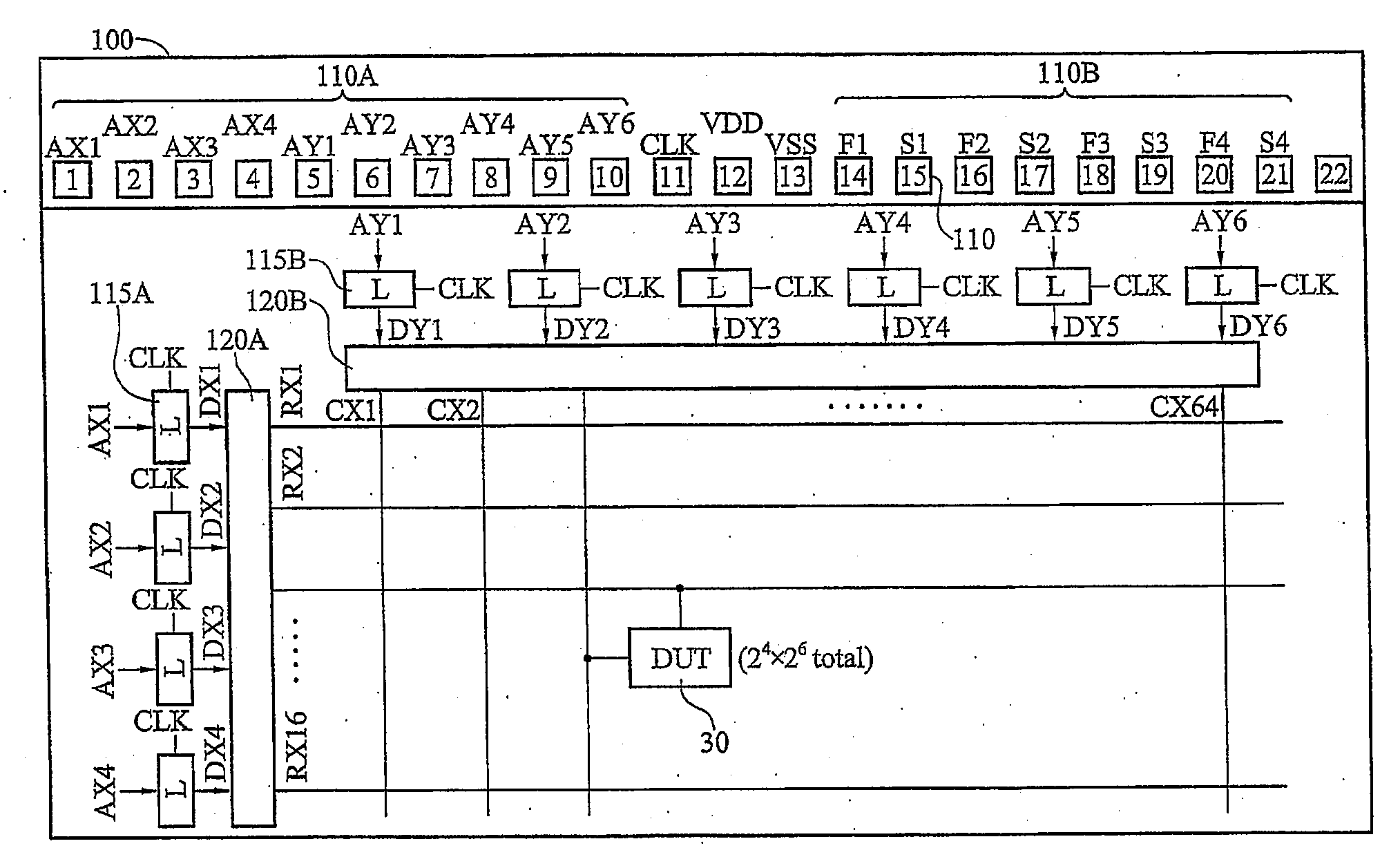
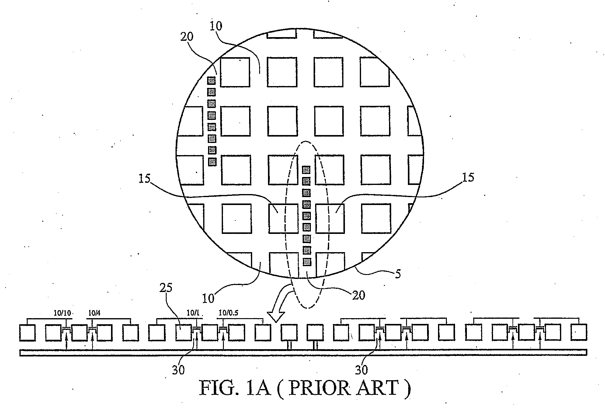
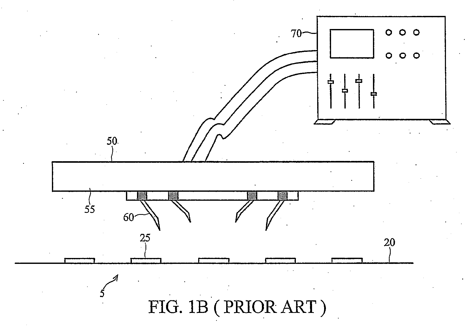
[0026]The present invention will be described with respect to preferred embodiments in a specific context, namely a high accuracy and universal device-under-test (DUT) on-chip switch matrix testline (MUX testline) for wafer acceptance testing (WAT). The preferred embodiments of the invention include the MUX testline structure and testing methodology using the testline structure. The invention may also be applied, however, to benefit other R&D activities, such as yield analysis, design-of-experiment (DOE), statistical split, and customized user test key input, among others.

[00...


PUM


Abstract

A testline structure made for integrated circuit tests is presented. The structure includes an array of testline pads formed in the scribe line area or integrated circuit die area on a semiconductor substrate, a plurality of test devices formed under the pads area, and a select circuit selectively connecting one of the test devices. The testline structure of this invention enables access to a large number of test devices through the same number of pads as on a conventional testline and can be employed to conduct parametric, reliability, and functional tests on the same. A source measurement unit (SMU) in a conventional integrated circuit tester is employed to sense and force predetermined test conditions on the test device terminals and conduct accurate Kelvin tests on the selected device. A method of using this testline structure is also presented.

Description

CROSS-REFERENCE TO RELATED APPLICATIONS[0001]This application relates to the following co-pending and commonly assigned U.S. patent application Ser. No. ______, filed Mar. 30, 2007, entitled “Network Based Integrated Circuit Testline Generator” (Attorney Docket No. TSM06-0412D).TECHNICAL FIELD[0002]The present invention relates generally to the testing of integrated circuits, and more particularly to the making and using of a high accuracy and universal switch matrix testline on integrated circuit wafer substrate for wafer acceptance testing (WAT) and other R&D testing needs.BACKGROUND[0003]In integrated circuit (IC) manufacturing, a semiconductor wafer typically contains a plurality of testlines in the scribe line area between adjacent wafer dies. Each testline includes a number of test devices, which are devices similar to those that are normally used to form the integrated circuit products in the wafer die area. By studying the parametric test results of devices on these testline...

Claims


Application Information

Patent Timeline
Patent Type & Authority Applications(United States)
IPC IPC(8): G01R31/02
CPCG01R31/2831G01R31/2884G01R31/2891H01L2924/0002H01L2924/00
Inventor LO, TSENG CHINLI, KUO-TSAIWU, SHIEN-YANG
Owner TAIWAN SEMICON MFG CO LTD
Why Eureka
Try Eureka