Image sensor module with a three-dimensional die-stacking structure

a technology of image sensor module and die-stacking structure, which is applied in the direction of electrical equipment, semiconductor devices, semiconductor/solid-state device details, etc., can solve the problems of large package size, inability to meet the needs of future products, and large electrical connection length, so as to reduce the electrical connection length of the image sensor module

Active Publication Date: 2008-12-18
IND TECH RES INST
View PDF11 Cites 106 Cited by
  • Summary
  • Abstract
  • Description
  • Claims
  • Application Information

AI Technical Summary

Benefits of technology

[0006]The present invention provides an image sensor module with a three-dimensional die-stacking structure. The image sensor module includes at least one image sensor die and at least one image processor die underlying it. By employing vertical electrical conductive wires within the image sensor die, vertical and horizontal electrica

Problems solved by technology

As described above, a conventional package structure for an image sensor typically employs a two-dimensional die-stacking structure and connection, which results in a greater electrical connection len

Method used


Image

  • Image sensor module with a three-dimensional die-stacking structure
  • Image sensor module with a three-dimensional die-stacking structure
  • Image sensor module with a three-dimensional die-stacking structure

Examples


first embodiment

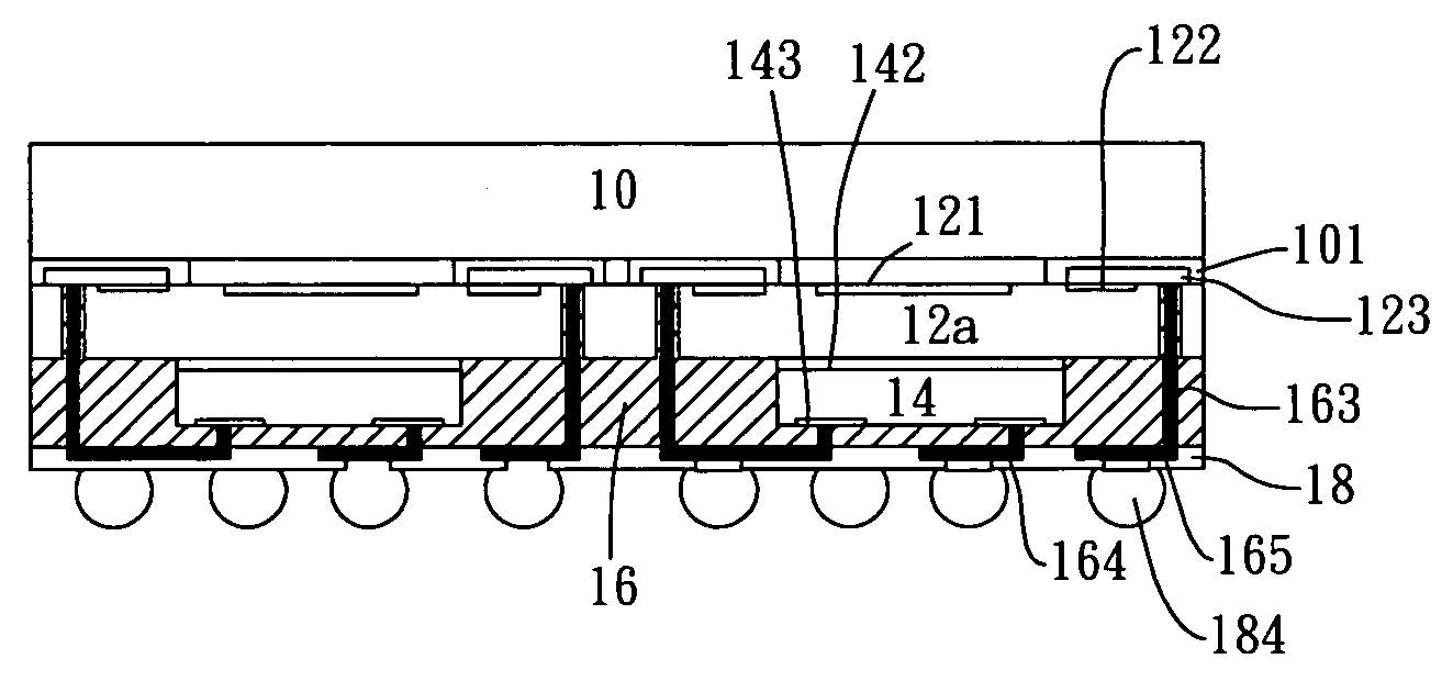
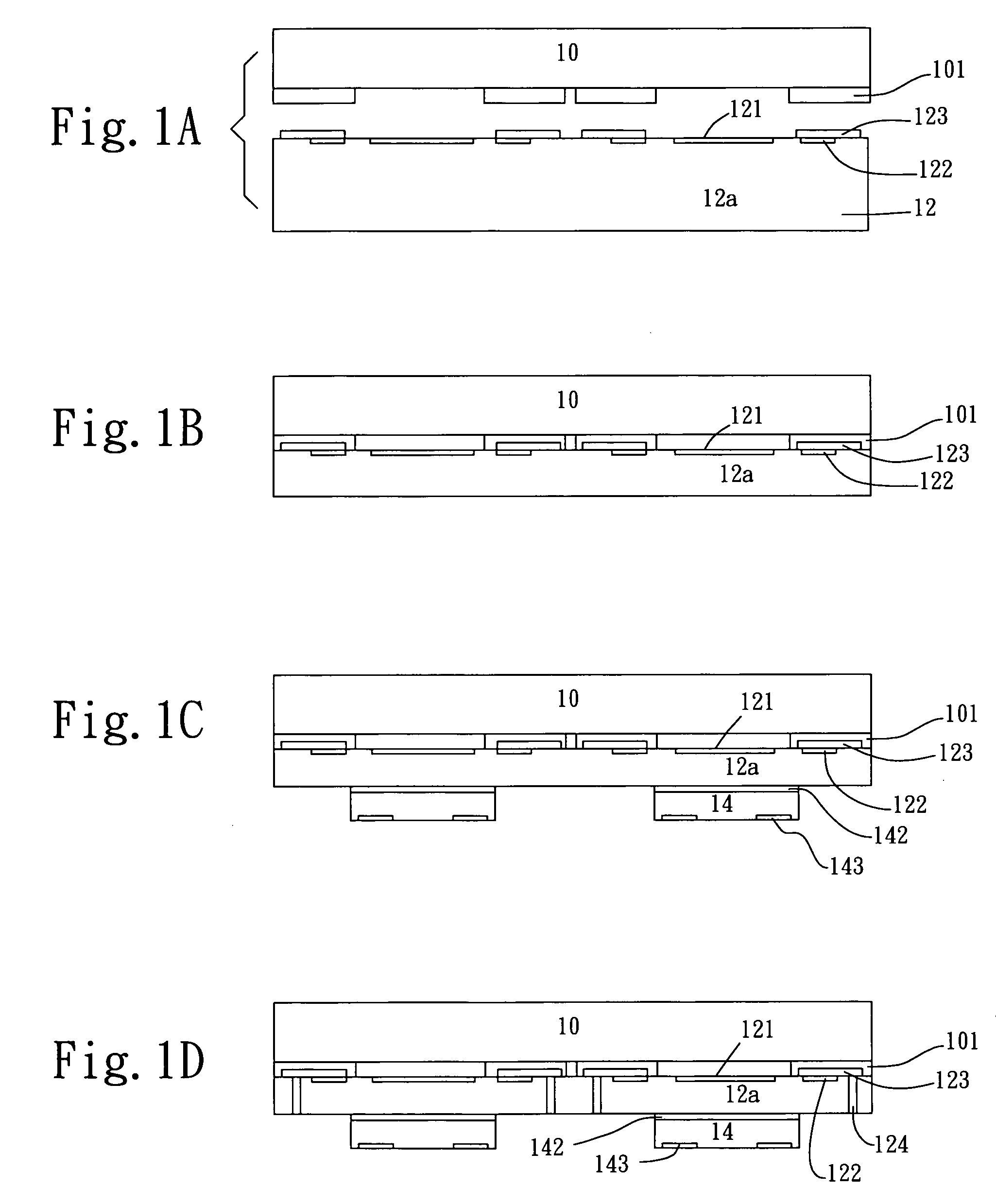
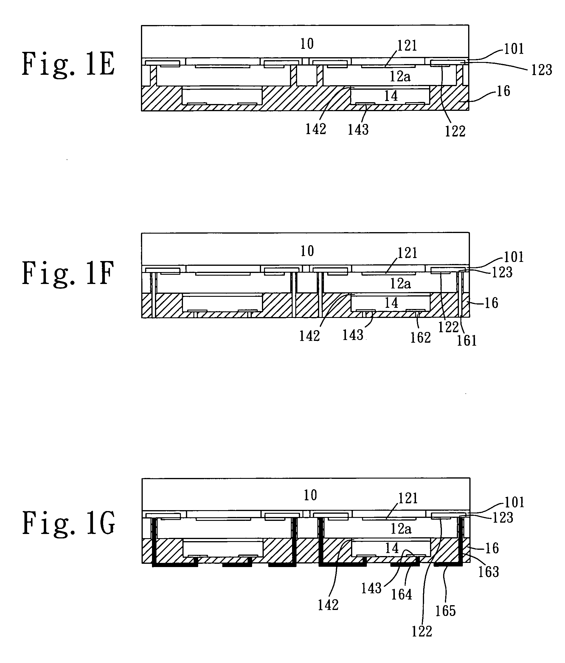
[0023]FIG. 2 is a schematic cross-sectional view of an image sensor module with a three-dimensional die-stacking structure in accordance with the invention. FIG. 1A through FIG. 1I is schematic cross-sectional views respectively corresponding to various stages in a process of forming the image sensor module 20 of FIG. 2. With reference to FIG. 1A first, an optically transparent substrate 10 and an image sensor wafer 12 are provided. The optically transparent substrate 10 can be made of glass or other polymer material. The image sensor wafer 12 includes a plurality of image sensor dies 12a, e.g., CMOS image sensor dies. Each of the image sensor dies 12a has a light sensitive area 121 and a plurality of metal layers 122, which are formed on an upper surface of the image sensor die 12a. A plurality of metal pads 123, e.g., aluminum pads, is formed correspondingly under each of the metal layers 122 within the image sensor die 12a, and electrically contacting the metal layers 122. The pr...

eighth embodiment

[0029]FIG. 9 is a schematic cross-sectional view of an image sensor module with a three-dimensional die-stacking structure in accordance with the invention. In this illustrated embodiment, the image sensor module 90 of the invention includes an optically transparent substrate 10, an image sensor die 901 with image processing capabilities, a SOC die 905 integrating memories, RF components and IPDs (Integrated Passive Devices), an insulating material 16, a protective layer 18, and a plurality of solder bumps 184. The image sensor die 901 has a light sensitive area 121 jointed to a bottom of the optically transparent substrate 10 by using an adhesive layer 101. The SOC die 905 is buried in the insulating material 16 and jointed to a backside of the image sensor die 901 by using a die attach film 142. The protective layer 18 is formed under the image sensor die 901, and the solder bumps 184 are formed at the pad openings (not shown) of the protective layer 18. With the solder bumps 184,...


PUM


Abstract

This invention provides an image sensor module with a three-dimensional die-stacking structure. By filling a conductive material into through silicon vias within at least one image sensor die, and into via holes within an insulating layer, vertical electrical connections are formed between the image sensor die and an image processor buried in the insulating layer. A plurality of solder bumps is formed on a backside of the image sensor module so that the module can be directly assembled onto a circuit board. The image sensor module of this invention is characterized by a wafer-level packaging architecture and a three-dimensional die-stacking structure, which reduces electrical connection lengths within the module and thus reduces an area and height of the whole packaged module.

Description

BACKGROUND OF THE INVENTION[0001]1. Field of the Invention[0002]The present invention relates to a package structure for an image sensor module, and more particularly to a package structure for an image sensor module with a three-dimensional die-stacking structure.[0003]2. Description of the Related Art[0004]Image sensors have been widely applied to electronic devices like camera cell phones, digital cameras, and devices associated with medical diagnoses or security monitoring. There are always needs on the market for thinner and more compact devices wherein energy loss can be reduced and production cost can be lowered, especially when portable electronic devices or medical instruments are considered. There are several known types of package structure for an image sensor: FIG. 11A of U.S. Pat. No. 6,646,289 discloses a wafer-level package structure for an image sensor, which employs a redistributed layer to redistribute electrical connections from the edge to the backside surface of...

Claims


Application Information

Patent Timeline
IPC IPC(8): H01L23/34
CPCH01L25/0657H01L25/16H01L27/14618H01L27/14634H01L2223/6677H01L2225/06527H01L2225/06541H01L2225/06582H01L2924/19103H01L2924/19104H01L24/19H01L24/24H01L24/97H01L2224/12105H01L2224/24145H01L2224/32145H01L2224/73267H01L2224/92244H01L2224/97H01L2924/00H01L2924/15311H01L2224/83H01L2224/82H01L2924/12041H01L2224/05008H01L2224/05026H01L2224/0557H01L2224/05001H01L2224/051H01L2924/00014H01L2224/05571H01L2224/05599
Inventor CHANG, SHU-MINGKUO, TZU-YINGCHIANG, CHIA-WENCHANG, HSIANG-HUNG
Owner IND TECH RES INST
Why Eureka
Try Eureka