Semiconductor memory device having memory cell and reference cell connected to same sense amplifier and method of reading data thereof

a memory device and memory cell technology, applied in the direction of information storage, static storage, digital storage, etc., can solve problems such as data reading errors, and achieve the effect of suppressing the potential fluctuation of the potential lin

Inactive Publication Date: 2008-12-18
RENESAS ELECTRONICS CORP
View PDF4 Cites 2 Cited by
  • Summary
  • Abstract
  • Description
  • Claims
  • Application Information

AI Technical Summary

Benefits of technology

[0023]Accordingly, in a case where the lowering of the potential of the potential line for supplying the reference potential to the reference cell occurs, charges are supplied from the dummy cell to the potential line. On the other hand, in a case where the potential increase of the potential line occurs, charges are discharged from the potential line to the dummy cell. This can suppress the potential fluctuation of the potential line. Accordingly, even in a high speed operation, it is possible to prevent reading of the data from the memory cell in a state where the potential of the reference cell is apart from a predetermined reference potential.
[0024]According to the present invention, a semiconductor memory device excellent in the reliability upon data reading, and a data reading method thereof are attained.
[0028]Accordingly, in a case where the lowering of the potential of the potential line for supplying the reference potential to the first reference cell occurs, charges are supplied from the second reference cell to the potential line. On the other hand, in a case where the potential increase of the potential line occurs, charges are discharged from the potential line to the second reference cell. This can suppress the potential fluctuation of the potential line. Accordingly, even in a high speed operation, it is possible to prevent reading of the data from the memory cell in a state where the potential of the first reference cell is apart from a predetermined reference potential.
[0029]According to the present invention, a semiconductor memory device excellent in the reliability upon data reading, and a data reading method thereof are attained.

Problems solved by technology

This leads to an error for the data reading.

Method used


Image

  • Semiconductor memory device having memory cell and reference cell connected to same sense amplifier and method of reading data thereof
  • Semiconductor memory device having memory cell and reference cell connected to same sense amplifier and method of reading data thereof
  • Semiconductor memory device having memory cell and reference cell connected to same sense amplifier and method of reading data thereof

Examples


first embodiment

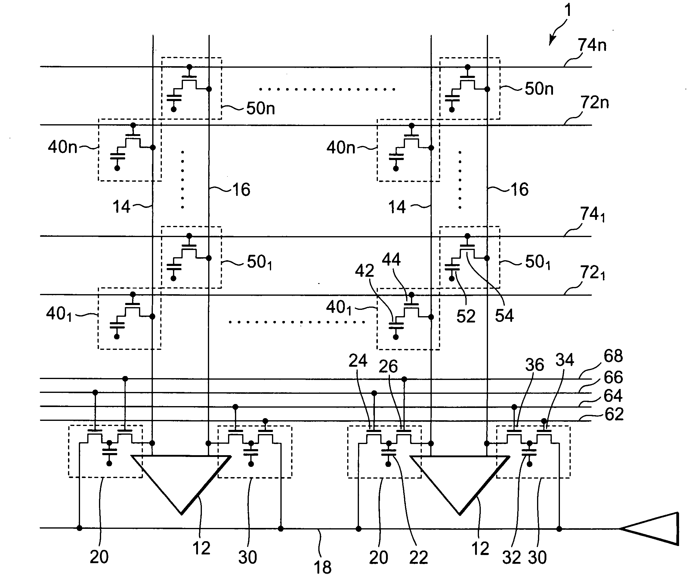
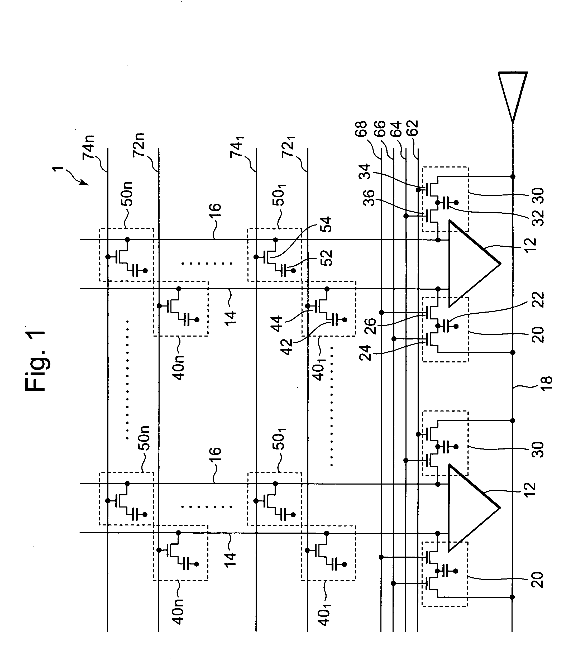
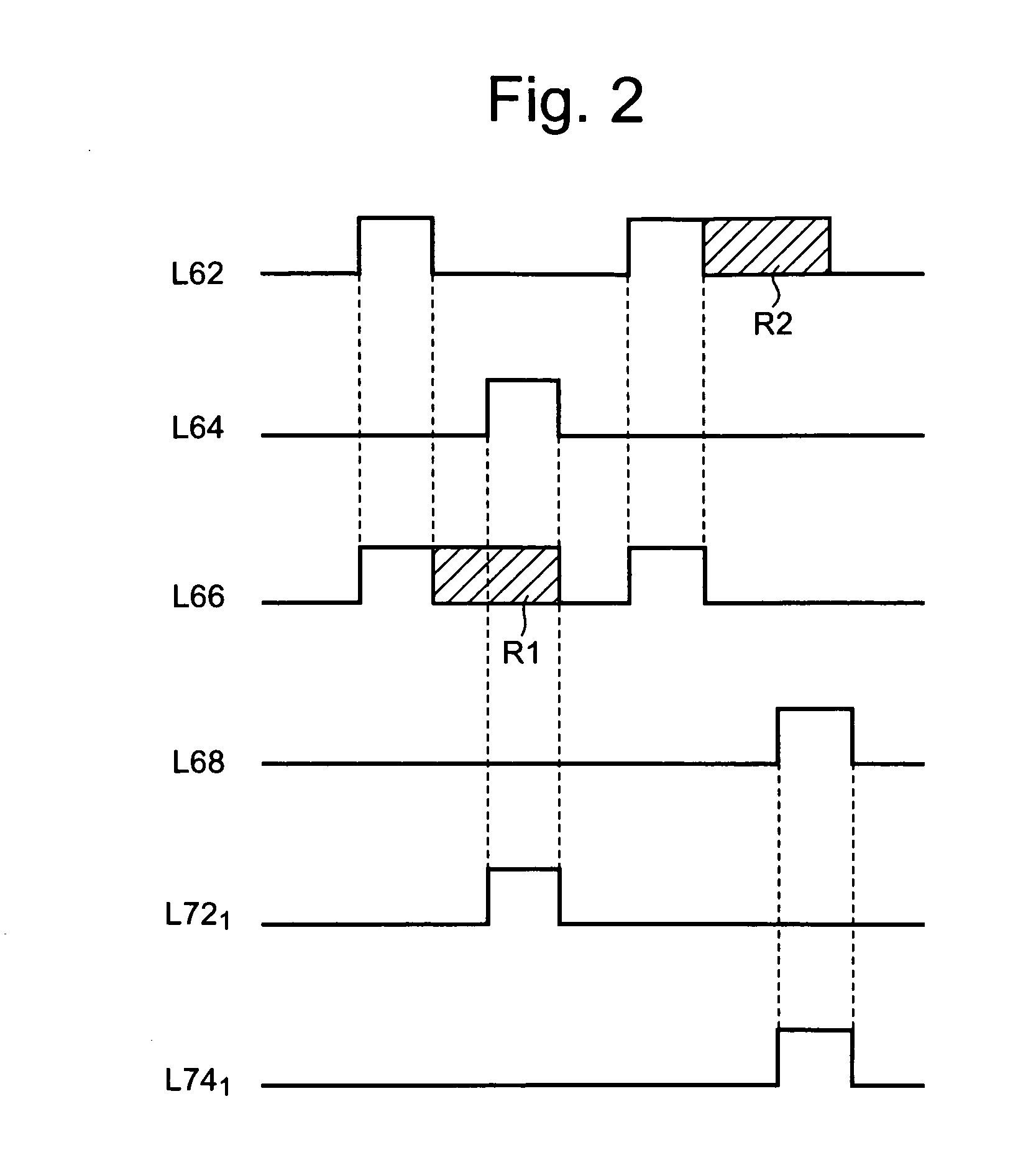
[0046]FIG. 1 is a circuit diagram showing the first exemplary embodiment of a semiconductor memory device according to the present invention. DRAM 1 is a semiconductor memory device of conducting reading of data by comparison between the potential of a memory cell and a reference potential of a reference cell and includes a bit line 14 (first bit line), a bit line 16 (second bit line), a reference cell 20 (first reference cell), and a reference cell 30 (second reference cell). DRAM 1 is constituted such that writing of the reference potential to the reference cell 20 and the reference cell 30 is started simultaneously. Specifically, the semiconductor memory device is provided with a control circuit, having a function for controlling such a timing that a later described word line 66 (first word line) and a word line 62 (second word line) are activated simultaneously. The control circuit is, for example, provided in the DRAM 202 or the logic circuit 206 of FIG. 10.

[0047]The bit line 1...

second embodiment

[0063]FIG. 3 is a circuit diagram showing the second exemplary embodiment of the semiconductor memory device according to the present invention. In DRAM 2, a word line 62 and a word line 66 are connected with each other via a wring 63. In this embodiment, writing a reference potential to a reference 20 and a reference 30 is therefore started simultaneously and ended simultaneously. Other constitutions and behaviors of DRAM 2 are identical with those of DRAM 1.

[0064]In this embodiment, mutual connection between the word lines 62 and 66 facilitates writing of the reference potential to the reference cells 20 and 30 simultaneously. Since this embodiment needs no control circuit that controls a time to write a reference potential to both reference cells 20 and 30, the circuit configuration of DRAM 2 is simplified by just that much. This contributes to size and cost reduction of the DRAM 2. Other effects of this embodiment are identical with those of the first embodiment.

third embodiment

[0065]FIG. 4 is s circuit diagram showing a third exemplary embodiment of a semiconductor memory device according to the present invention. In DRAM 3 is provided with a word line 65 in place of a word line 62 and a word line 66 (see FIGS. 1 and 3). That is, the gates of transistors 24 and 34 are connected to a common word line 65. In this embodiment, writing a reference potential to a reference 20 and a reference 30 is therefore started simultaneously and ended simultaneously. Other constitutions and behaviors of DRAM 3 are identical with those of DRAM 1.

[0066]In this embodiment, connection of the gates of transistors 24 and 34 to a common word line 65 facilitates writing of a reference potential simultaneously to reference cells 20 and 30. Since this embodiment needs no control circuit that controls a time to write the reference potential to both the reference cells 20 and 30, the circuit configuration of DRAM 3 is simplified by just that much. This contributes to size and cost red...


PUM


Abstract

A semiconductor memory device includes a sense amplifier, first and second bit lines connected to the sense amplifier, a first reference cell connected to the first bit line, and a second reference cell connected to the second bit line. A reference potential is simultaneously written to the first and second reference cells. Further, a dummy cell may be provided to be simultaneously, with the reference cell, with the reference potential.

Description

BACKGROUND OF THE INVENTION[0001]1. Field of the Invention[0002]The present invention relates to a semiconductor memory device and a data reading method thereof. Particularly, it relates to a semiconductor memory circuit constituting a logic embedded memory in which a semiconductor memory circuit is embedded on a substrate identical with that for the logic circuit, as well as a data reading method thereof.[0003]2. Description of Related Art[0004]FIG. 10 is an example of a logic embedded memory. A logic circuit 206 and other peripheral circuits (high speed IO circuit 208, AD converter 210, DA converter 212) are disposed on a substrate identical with that for a semiconductor memory device such as DRAM 202 or SRAM 204. For the semiconductor memory circuit in the logic embedded memory described above, high speed operation is required in comparison with existent general-purpose semiconductor memory circuits.[0005]On the other hand, FIG. 11 is a circuit diagram showing an existent semicon...

Claims


Application Information

Patent Timeline
Patent Type & Authority Applications(United States)
IPC IPC(8): G11C7/00
CPCG11C11/4091G11C11/4099
Inventor SAKOH, TAKASHI
Owner RENESAS ELECTRONICS CORP
Why Eureka
Try Eureka