
Process for producing a functional device-mounted module

a functional device and module technology, applied in semiconductor lasers, semiconductor/solid-state device details, lasers, etc., can solve the problems of limited heat dissipation properties, high cost of conventional modules, and limited ability to reduce in size of conventional modules, so as to achieve excellent heat dissipation properties and largely downsize

Inactive Publication Date: 2008-12-18
SONY CORP
View PDF3 Cites 2 Cited by
  • Summary
  • Abstract
  • Description
  • Claims
  • Application Information

AI Technical Summary

Benefits of technology

The present patent relates to a functional device-mounted module comprising a substrate with a wiring pattern, a functional device mounted on the substrate, and a package component member sealed with resin. The invention provides a method for protecting the function part of the functional device during assembly, a protecting cover member for the package component member, a gas exhaust member for improving reflowing resistance, and a damming portion to improve the quality and yield of the product. The invention also allows for the use of a protecting cover member that is releasable from the package component member. The functional device-mounted module provides a compact and efficient solution for mounting functional devices on a substrate.

Problems solved by technology

Therefore, the conventional module becomes very expensive.
Further, in order to simultaneously transmit another wavelength (for example, 780 nm for CD applications and 650 nm for DVD applications), a more expensive coating needs to be applied.
Thus, the conventional module is limited in its ability to be reduced in size.

Method used


Image

  • Process for producing a functional device-mounted module
  • Process for producing a functional device-mounted module
  • Process for producing a functional device-mounted module

Examples


Embodiment Construction

[0050]In the following, preferred embodiments of the present disclosure will be explained in detail with reference to the drawings.

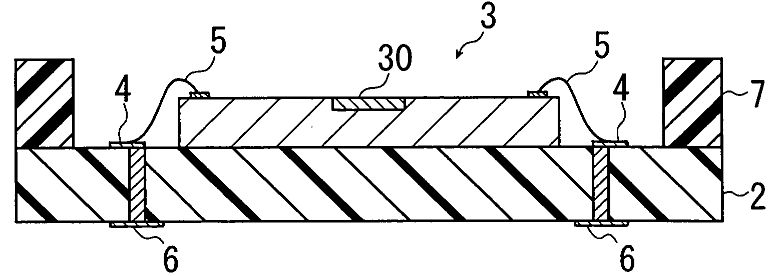
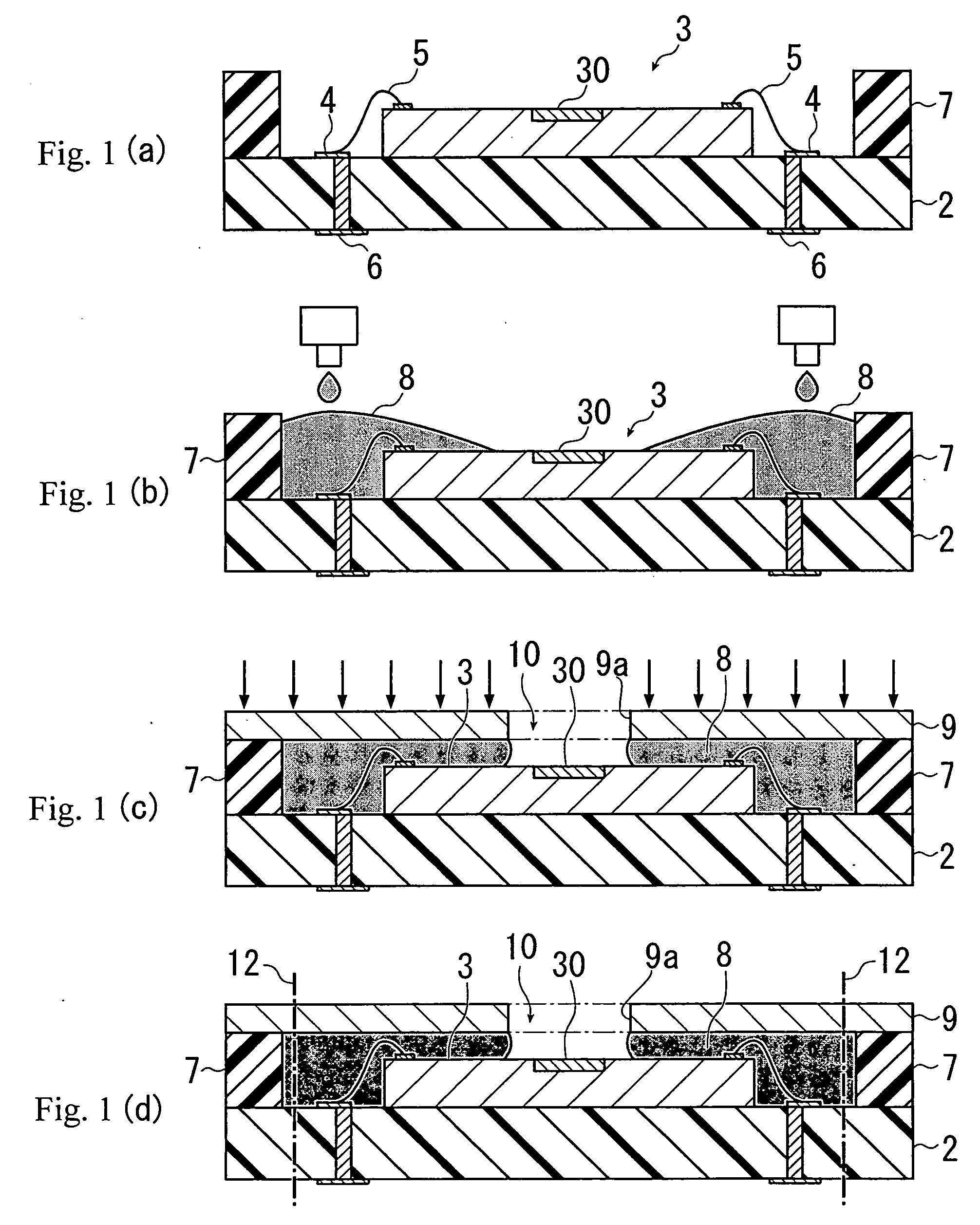
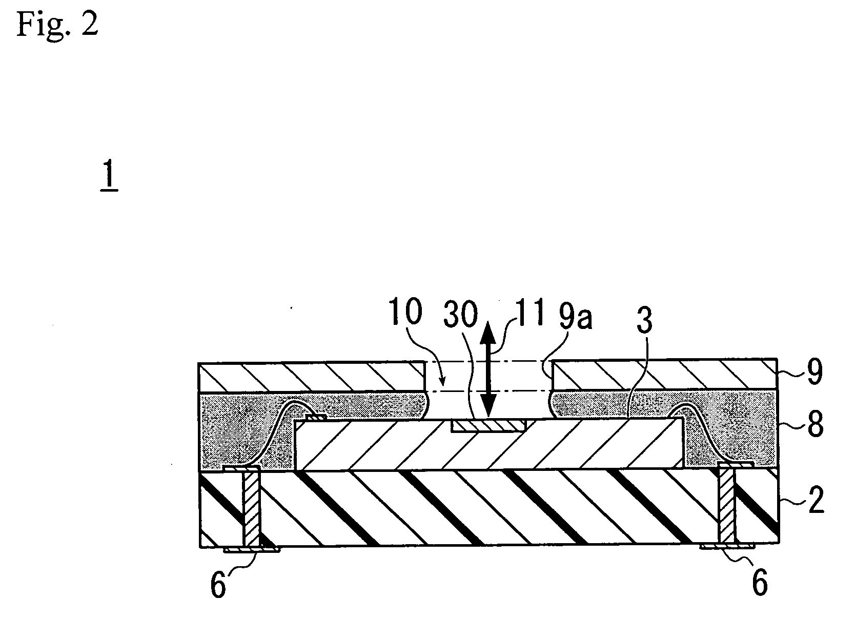
[0051]FIGS. 1(a) to (d) are sectional construction views showing an exemplary embodiment of the process for producing the optical functional device-mounted module according to the present disclosure. FIG. 2 is a sectional construction view showing an embodiment of the same optical functional device-mounted module.

[0052]As shown in FIG. 1(a), according to this embodiment, an optical functional device 3 having an optical function part (function part) 30, such as a light receiving element or a light emitting element is first mounted on a substrate having a prescribed wiring pattern 4.

[0053]In this embodiment, contact portions of the wiring pattern 4 on the substrate 2 are electrically connected to those of the optical functional device 3 by gold wires 5, and current flows through external connecting terminals 6 at a back side of the substrate 2.

[0054]A bank...


PUM


Abstract

The present disclosure provides an optical functional device-mounted module which needs no expensive or special members, can be reduced in size, and provide a producing process thereof. A bank to dam a liquid sealing resin is provided on a substrate around an optical functional device, the substrate being formed with a predetermined wiring pattern and having the optical functional device mounted thereon. The liquid sealing resin is filled between the functional device and the bank by dropping the liquid sealing resin therebetween. A package component member having a light transmission hole corresponding to an optical function part of the optical functional device is brought into contact with the bank such that the light transmission hole is opposed to the function part of the optical functional device, thereby causing the package component member to contact with the liquid sealing resin. The package component member is fixed onto the substrate by curing the liquid sealing resin and the bank is finally cut off and removed.

Description

CROSS-REFERENCE TO RELATED APPLICATIONS[0001]This is a Division of application Ser. No. 11 / 717,066 filed on Mar. 13, 2007, which is a Continuation of International Application No. PCT / JP2005 / 015406 filed Aug. 25, 2005. The disclosures of the prior applications are incorporated by reference herein in their entirety.BACKGROUND[0002]1. Field of the Invention[0003]The present invention relates to a functional device-mounted module such as a light receiving element and a light emitting element, for example. Particularly, the present invention relates to an optical functional device-mounted module in which an optical functional device is mounted on a substrate by using a sealing resin.[0004]2. Discussion of the Relevant Art[0005]Conventionally, for example, a module having a hollow structure is known in the art.[0006]As shown in FIG. 10, a package 101 of a conventional optical functional device-mounted module 100 is constructed by installing a light transmission member 104 on a substrate ...

Claims


Application Information

Patent Timeline
Patent Type & Authority Applications(United States)
IPC IPC(8): H01L21/00H01L21/56H01L31/02H01S5/022
CPCH01L23/3185H01L24/45H01L2924/1461H01L2924/1815H01L2224/48091H01L24/49H01L24/48H01S5/32341H01S5/02296H01S5/02228H01L31/0203H01L33/54H01L33/56H01L2224/45144H01L2224/48227H01L2224/49175H01L2224/8592H01L2924/01004H01L2924/01079H01L2924/16195H01L2924/3025H01S5/005H01S5/02216H01L2924/00014H01L2924/00H01L2924/12042H01L2224/05554H01L2924/16151H01L2924/10161H01S5/02234H01S5/02257
Inventor YONEDA, YOSHIHIROASADA, TAKAHIRO
Owner SONY CORP
Learn More