Methods and Apparatus for Semiconductor Memory Devices Manufacturable Using Bulk CMOS Process Manufacturing

Active Publication Date: 2008-12-25
GIGADEVICE SEMICON (HK) LTD
View PDF7 Cites 3 Cited by
  • Summary
  • Abstract
  • Description
  • Claims
  • Application Information

AI Technical Summary

Benefits of technology

[0014]An advantage of the present invention is that it provides a semiconductor device capable of holding information where the semiconductor device can be manufactured using logic process of manufacturing.
[0015]Another advantage of the present invention is that it provides a semiconductor device manufacturable using logic process of manufacturing and operable as a memory device.
[0016]Yet another ad

Problems solved by technology

Thus, for certain applications, the space required on a die for the memory block can be quite significant.
For example, many system-on-a-chip applications require large blocks of memory cells, requiring large real estate on the die and an expensive application.
However, given the 6-transister (and 4-transister) memory cell structure, it is difficult to shrink t

Method used


Image

  • Methods and Apparatus for Semiconductor Memory Devices Manufacturable Using Bulk CMOS Process Manufacturing
  • Methods and Apparatus for Semiconductor Memory Devices Manufacturable Using Bulk CMOS Process Manufacturing
  • Methods and Apparatus for Semiconductor Memory Devices Manufacturable Using Bulk CMOS Process Manufacturing

Examples


Embodiment Construction

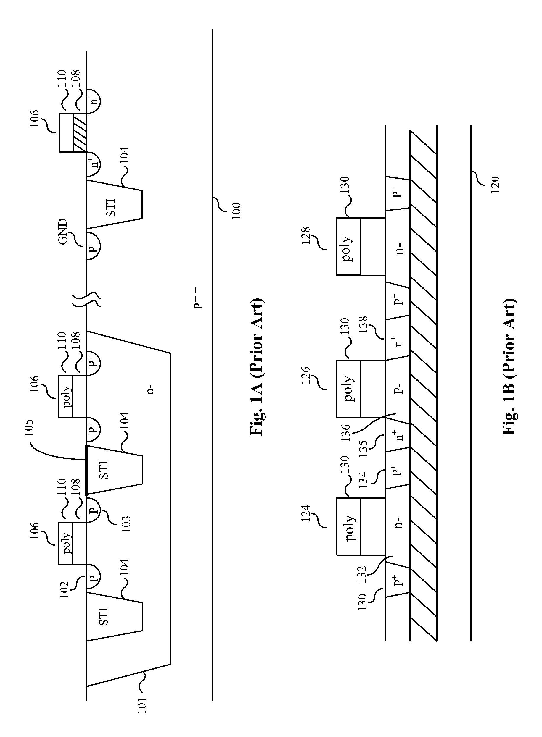
[0028]The present invention will now be described in detail with reference to preferred embodiments as illustrated in the accompanying figures. During the description, specific details are set forth in order to provide a thorough understanding of the present invention. However, it will be apparent to one skilled in the art that the present invention may be practiced without some or all of the specific details. In order to not unnecessarily obscure the present invention, some well know process steps or structures may not have been described in detail. In one embodiment, the present invention relates to semiconductor memories, and more particularly to memories and structures of such which provide efficient fabrication and functionality of the memories using preferred logic process of manufacturing.

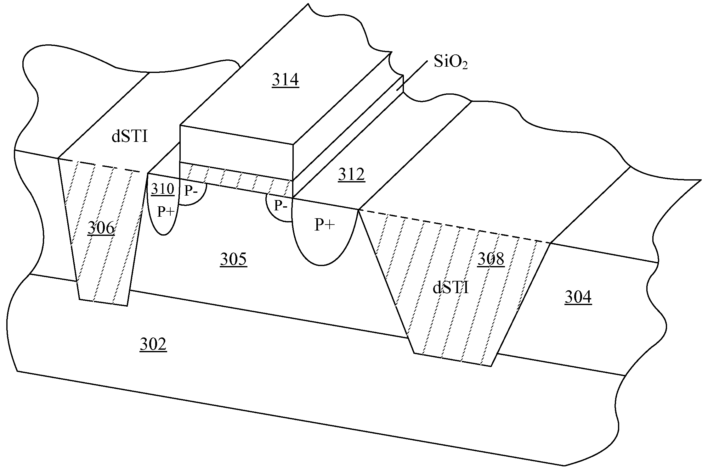
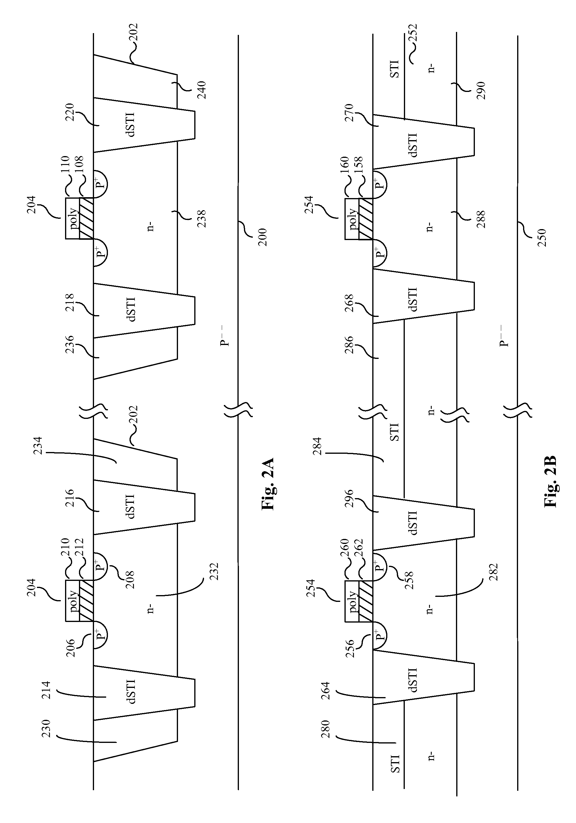
[0029]Referring to FIG. 2a, a presently preferred embodiment of the present invention is illustrated, where there is a substrate 200 and wells 202 deposited on the substrate 200. Each of the...


PUM


Abstract

The present invention discloses semiconductor devices that can be manufactured utilizing standard process of manufacturing and that can hold information. In accordance with a presently preferred embodiment of the present invention, one or more semiconductor devices can be formed in a well on a substrate where isolation trenches surround one or more devices to create storage regions (floating wells) that is capable of holding a charge. Depending on the charge in the storage region (floating well), it can represent information. The semiconductor devices of the present invention can be manufactured using the standard process of manufacturing (bulk cmos processing).

Description

CROSS REFERENCE[0001]This application claims priority from a patent application entitled “______ ” filed on ______ , having an application Ser. No. ______ . This application is incorporated herein by reference.FIELD OF INVENTION[0002]The present invention relates to semiconductor devices, in particular to semiconductor devices capable of storing information.BACKGROUND[0003]In the manufacturing of the semiconductor devices, a widely utilized and cost efficient type of manufacturing process offered by many foundries is the standard process (or bulk cmos processing). In standard process manufacturing of semiconductor devices, referring to FIG. 1a, as an illustration, a bulk substrate doped to be p−100 and one or more n− wells 101 may be deposited thereon. Within the well 101, one method of electrically isolating the active device regions is to form a trench isolation region 104 between adjacent devices 106. Such prior art trench isolation regions typically comprise a trench that is for...

Claims


Application Information

Patent Timeline
IPC IPC(8): H01L29/78H01L21/336
CPCH01L21/823878H01L21/823892H01L27/1052H10B99/00
Inventor ZHU, YIMING
Owner GIGADEVICE SEMICON (HK) LTD
Why Eureka
Try Eureka