

Method For Manufacturing Silicon Single Crystal Wafer
Inactive Publication Date: 2009-01-01
SHIN-ETSU HANDOTAI CO LTD
View PDF8 Cites 7 Cited by
- Summary
- Abstract
- Description
- Claims
- Application Information
AI Technical Summary
Benefits of technology
[0048]When such a method for manufacturing a silicon single crystal wafer according to the present invention is adopted, defects generated after the rapid thermal annealing can be annihilated in the subsequent heat treatment, and stable oxide precipitate nuclei can be formed in the bulk of the wafer during a device process. Moreover, a crystal region that can be used as a materia
Problems solved by technology
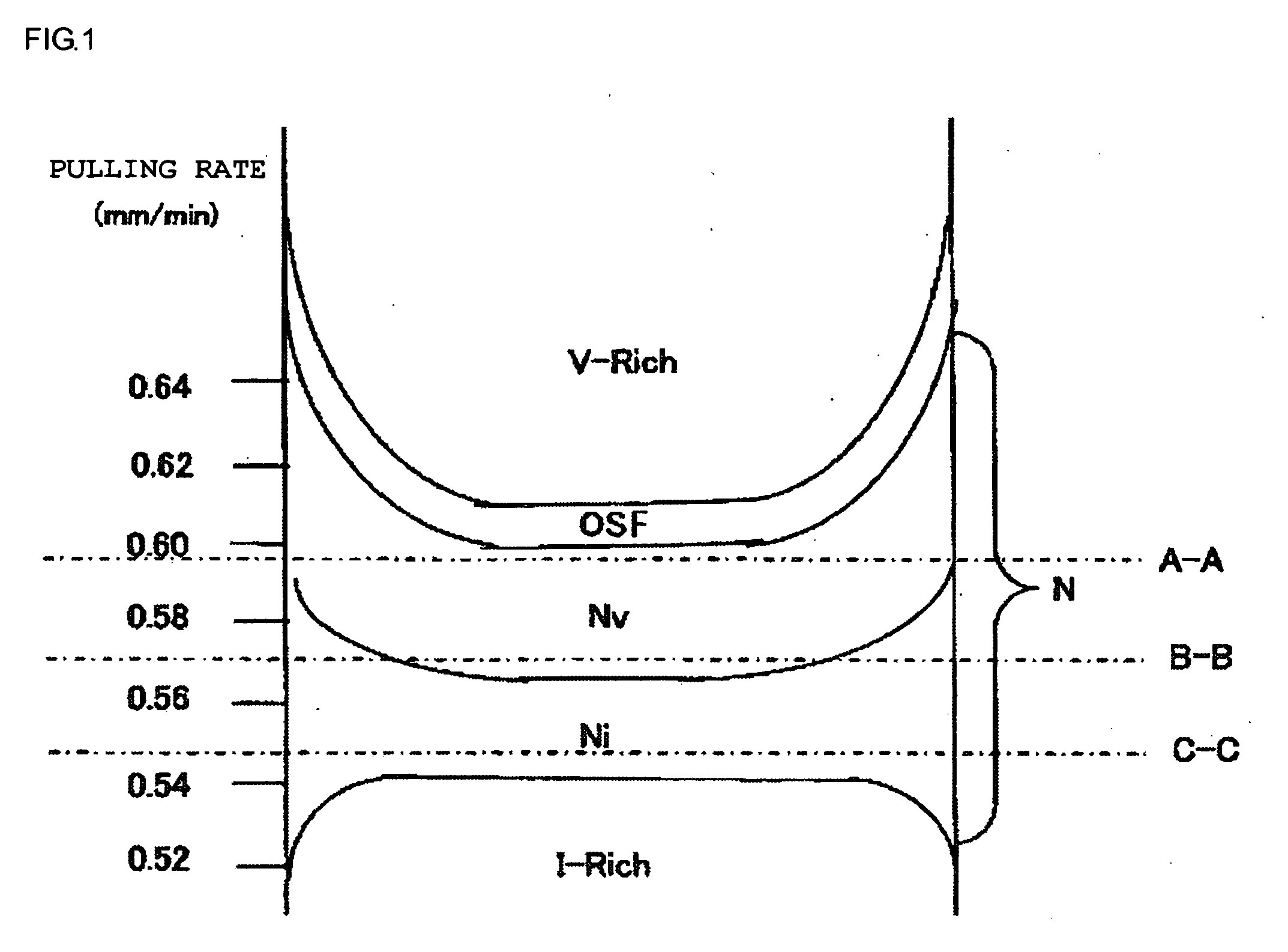
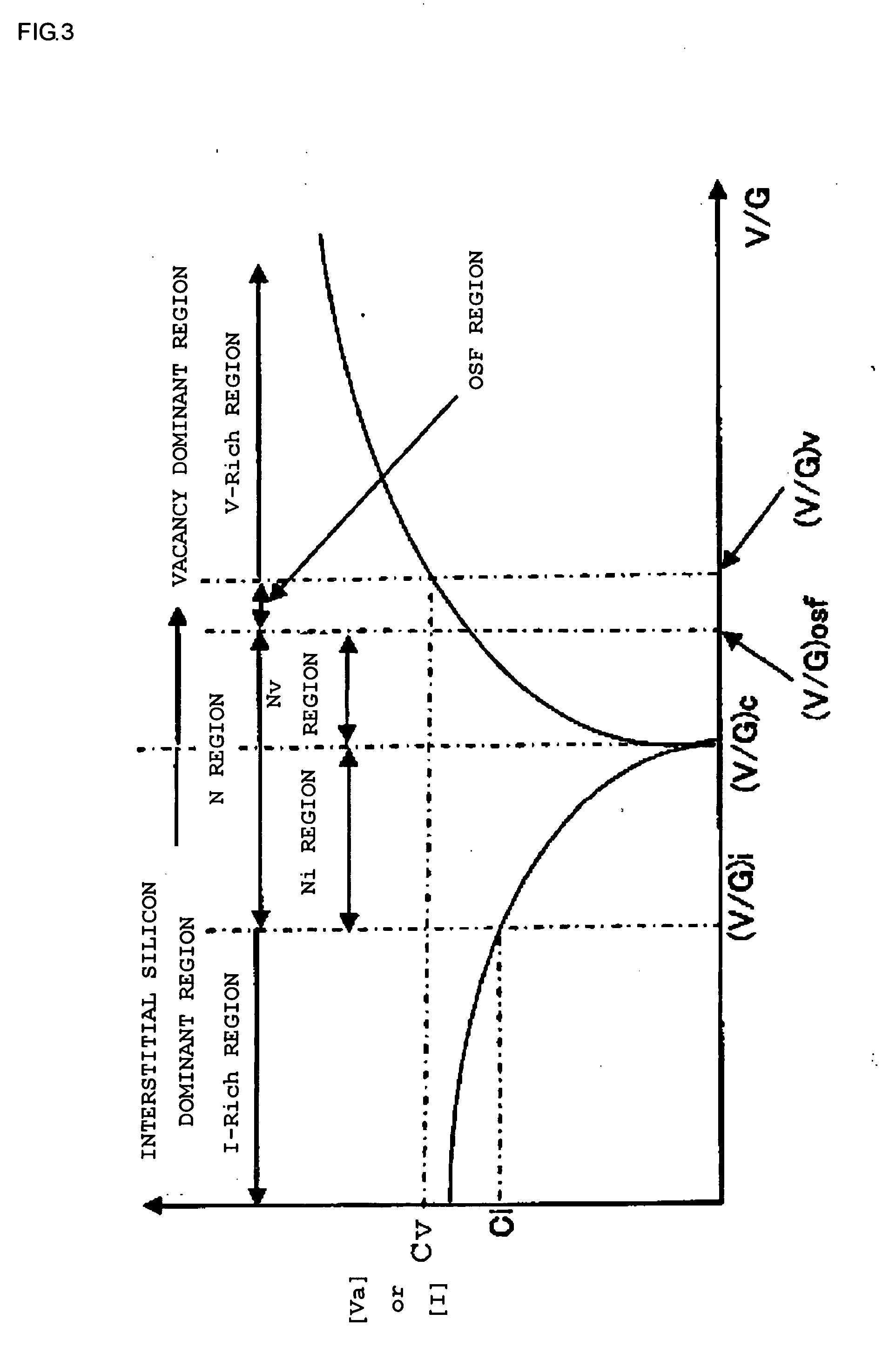
The silicon single crystal grown based on the CZ method in this manner may produce an oxidation induced stacking fault called OSF that is generated in a ring-like shape when subjected to a thermal oxidation treatment (e.g., at 1100° C. for two hours).
It has been revealed that a micro defect that is formed during crystal growth and adversely affects device performances (which will be referred to as a grown-in defect hereinafter) is present besides the OSF.
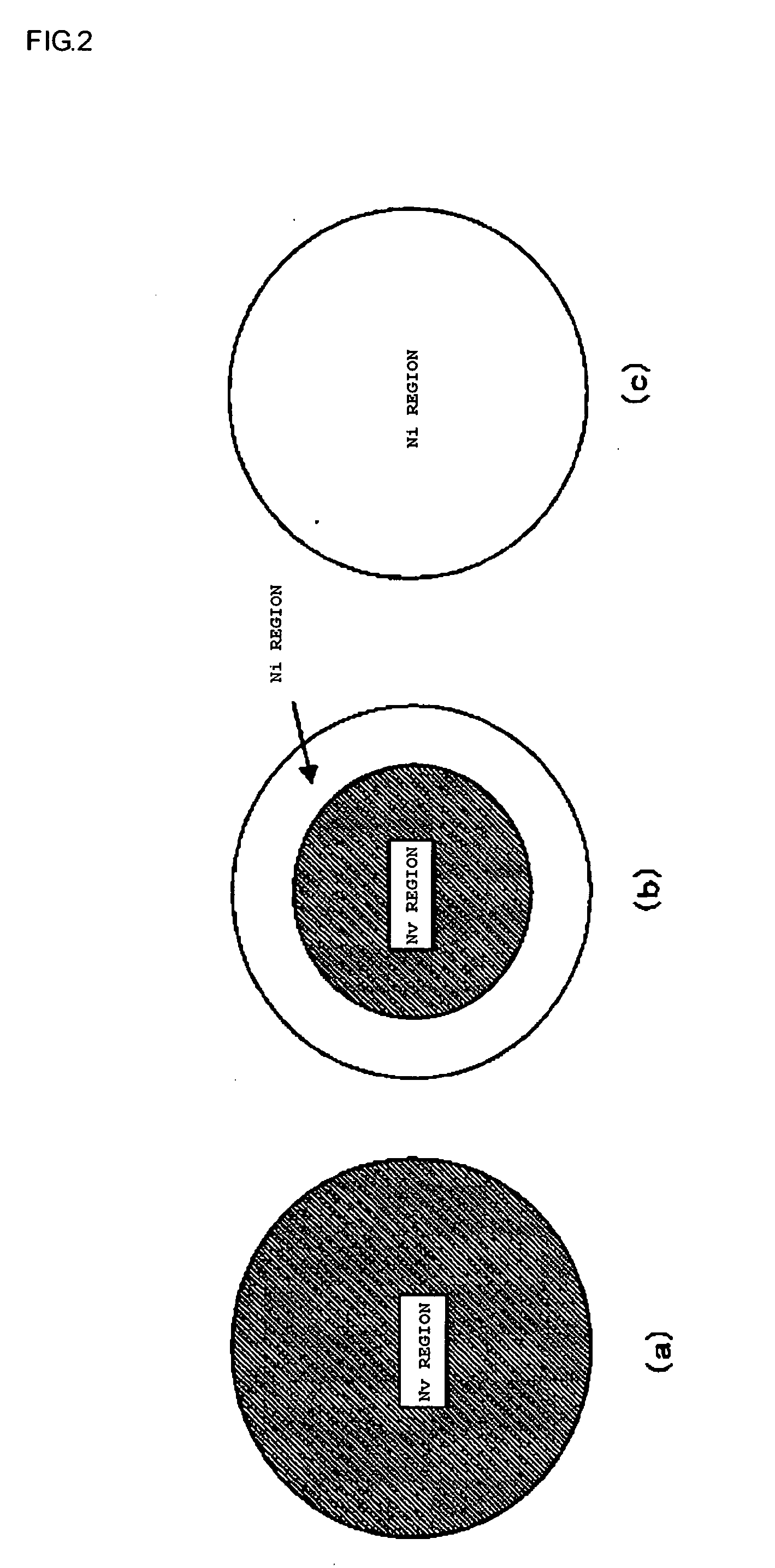
It has been revealed that, since this N region has unevenly distributed Va or I but has a saturated concentration or a lower concentration, an agglomerated defect like the COP or the FPD does not exist, or presence of the defect cannot be detected by a current defect detection method.
When Grown-in defects that are present in the V-Rich region or the I-Rich region appear on the wafer surface, such defects have an adverse effect, e.g., a reduction in an oxide dielectric breakdown voltage on device characteristics in a case where an MOS (Metal Oxide Semiconductor) structure of a device is formed, and hence no presence of such defects in a wafer surface layer is desired.
This BMD becomes a problem when it is generated in a device activation region in a wafer since the BMD adversely affects on device characteristics, e.g., junction leakage but, on the other hand, the BMD is effective when it is present in a bulk outside the device activation reg
Method used
View moreImage
Smart ImageViewing Examples

Examples
 PUM
 Abstract
The present invention provides a method for manufacturing a silicon single crystal wafer by which a silicon single crystal ingot is pulled based on a Czochralski method and a rapid thermal annealing is performed with respect to a wafer that is sliced out from the silicon single crystal ingot and has a whole area in a radial direction formed of N region, wherein a heat treatment at 800 to 1100° C. as a heat treatment temperature for two hours or below as a hear treatment time is carried out after the rapid thermal annealing while adjusting the heat treatment temperature and the heat treatment time so that at least diffusion distances of vacancies as point defects injected by the rapid thermal annealing become longer than diffusion distances of the vacancies by a heat treatment performed at 800° C. for 30 minutes, thereby annihilating a vacancy type defect. As a result, there is provided the manufacturing method capable of inexpensively manufacturing a silicon wafer that can assure a DZ layer with a sufficient thickness in a wafer front surface layer region and can also assure a sufficient quantity of oxide precipitates functioning as gettering sites in a bulk region on an earlier stage of a heat treatment in a device process.
Description
TECHNICAL FIELD[0001]The present invention relates to a method for manufacturing a silicon single crystal wafer that can form a DZ layer having no occurrence of crystal defects from a wafer surface to a fixed depth where a device activation region is formed and can form oxide precipitates serving as gettering sites in the wafer.BACKGROUND ART[0002]A silicon single crystal wafer that becomes a material of a semiconductor device can be generally fabricated by growing a silicon single crystal based on a Czochralski method (which will be referred to as a CZ method hereinafter) and applying processes such as slicing, polishing, the others to the obtained silicon single crystal ingot.[0003]The silicon single crystal grown based on the CZ method in this manner may produce an oxidation induced stacking fault called OSF that is generated in a ring-like shape when subjected to a thermal oxidation treatment (e.g., at 1100° C. for two hours). It has been revealed that a micro defect that is for...
Claims
Login to View More Application Information
Patent Timeline
 IPC IPC(8): C30B15/14
CPCC30B15/04C30B15/203H01L21/3225C30B33/02C30B29/06H01L21/20
InventorEBARA, KOJI
OwnerSHIN-ETSU HANDOTAI CO LTD