
Package stacking using unbalanced molded tsop

a technology of unbalanced molded tsop and stacking, which is applied in the direction of semiconductor devices, semiconductor/solid-state device details, electrical devices, etc., can solve the problems of faulty operation of multi-package assembly and more likely that respective packages may be dislodged from each other

Inactive Publication Date: 2009-01-01
SANDISK TECH LLC
View PDF4 Cites 15 Cited by
  • Summary
  • Abstract
  • Description
  • Claims
  • Application Information

AI Technical Summary

Benefits of technology

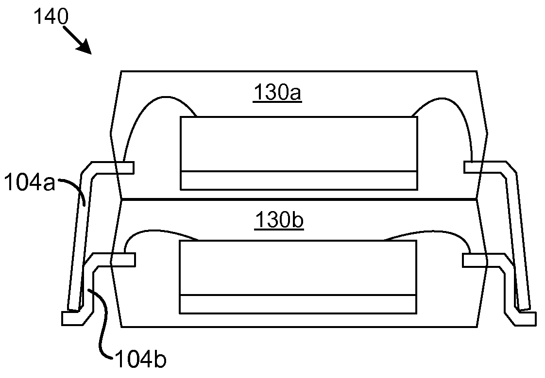
The present invention is about a method of making a semiconductor package assembly with two stacked semiconductor packages. The first package has a leadframe and semiconductor die attached to its leads, which are positioned near the bottom of the package. The first package is then placed on top of a second package, which can also be a leadframe-based package with leads that extend out of the mold compound. The two packages are securely bonded together using the overlap of the leads, which allows for a more secure mounting of the packages together. The technical effect of this invention is to provide a more robust and reliable semiconductor package assembly.

Problems solved by technology

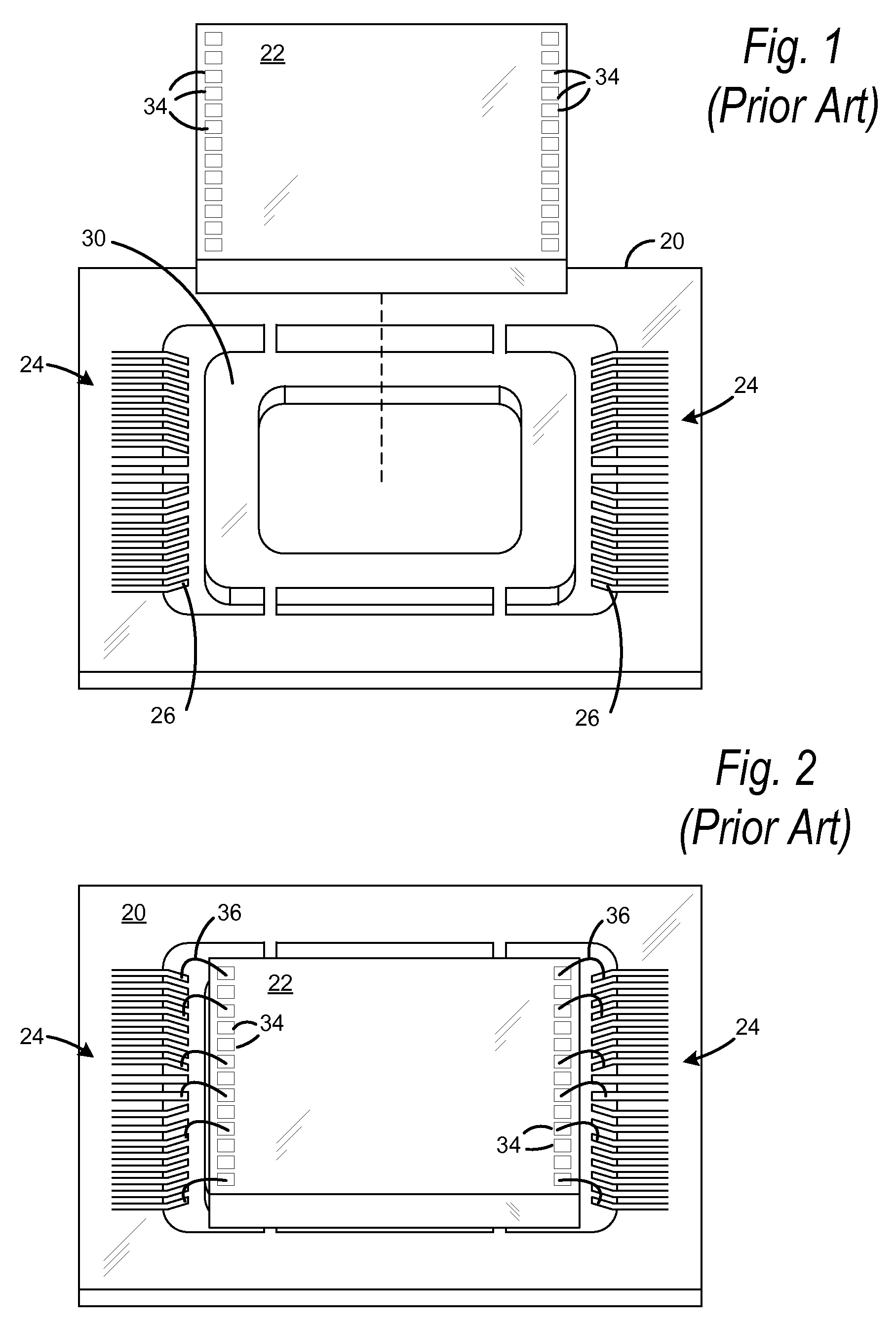
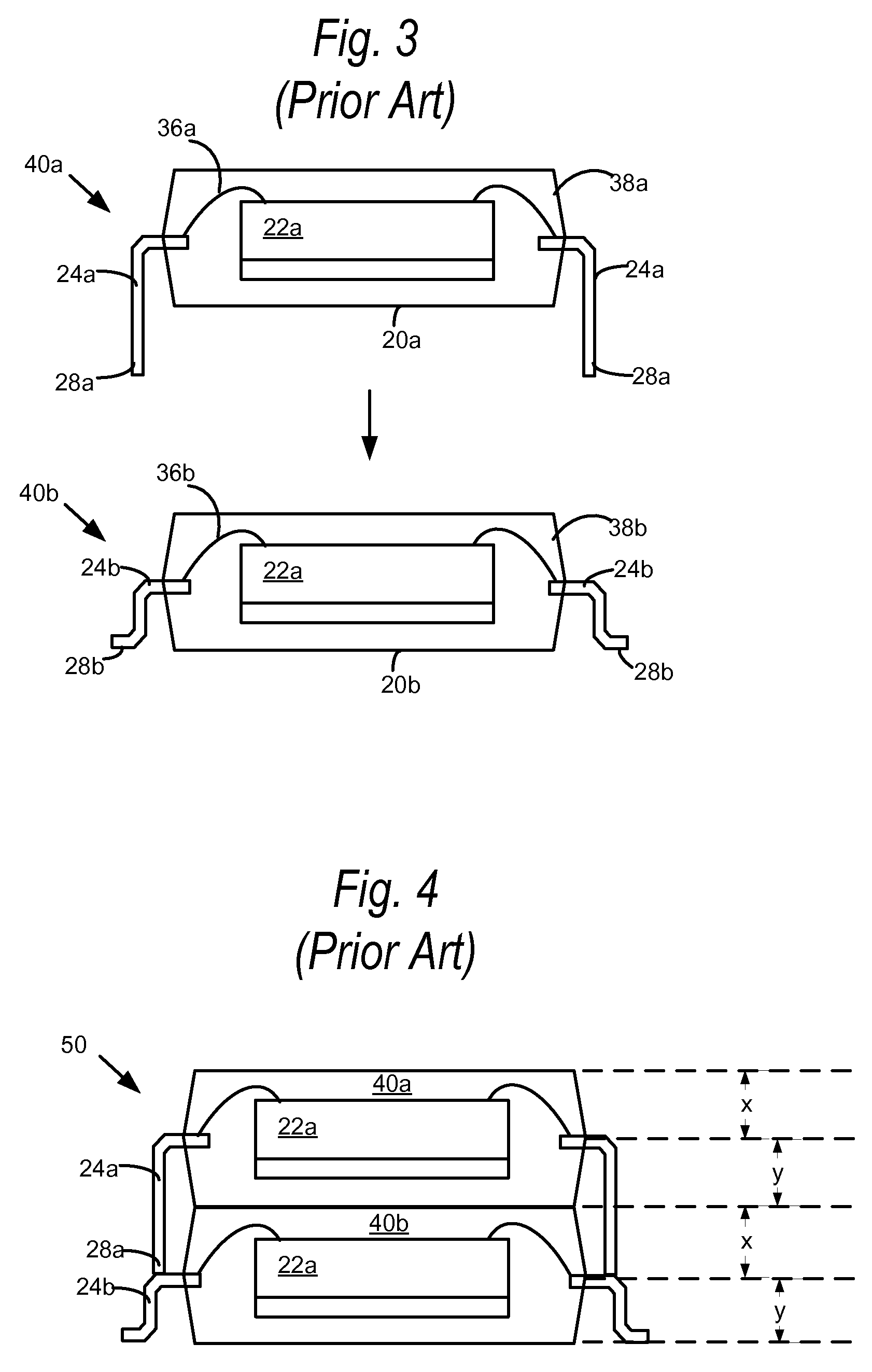
Such a small overlap can lead to unreliable bonding of certain leads of the respective packages to each other, and a potential faulty operation of the multi-package assembly.
Moreover, the small overlap makes it difficult to provide an adhesive between the respective semiconductor packages in the multi-package assembly, thus making it more likely that the respective packages may become dislodged from each other over time.

Method used


Image

  • Package stacking using unbalanced molded tsop
  • Package stacking using unbalanced molded tsop
  • Package stacking using unbalanced molded tsop

Examples


Embodiment Construction

[0026]Embodiments of the present invention will now be described in reference to FIGS. 5-9 which in general relate to a method of fabricating a semiconductor package, and a semiconductor package formed thereby. It is understood that the present invention may be embodied in many different forms and should not be construed as being limited to the embodiments set forth herein. Rather, these embodiments are provided so that this disclosure will be thorough and complete and will fully convey the invention to those skilled in the art. Indeed, the invention is intended to cover alternatives, modifications and equivalents of these embodiments, which are included within the scope and spirit of the invention as defined by the appended claims. Furthermore, in the following detailed description of the present invention, numerous specific details are set forth in order to provide a thorough understanding of the present invention. However, it will be clear to those of ordinary skill in the art th...


PUM


Abstract

A semiconductor package assembly is disclosed including a pair of stacked leadframe-based semiconductor packages. The first package is encapsulated in a mold compound so that the electrical leads emanate from the sides of the package, near a bottom surface of the package. The first package may be stacked atop the second package by aligning the exposed leads of the first package with the exposed leads of the second package and affixing the respective leads of the two packages together. The vertical offset of leads toward a bottom of the first package provides a greater overlap with leads of the second package, thus allowing a secure bonding of the leads of the respective packages.

Description

CROSS-REFERENCE TO RELATED APPLICATION[0001]The following application is cross-referenced and incorporated by reference herein in its entirety:[0002]U.S. patent application Ser. No. ______ [Attorney Docket No. SAND-01255US0], entitled “Method Of Package Stacking Using Unbalanced Molded TSOP,” by Ming Hsun Lee, et al., filed on even date herewith.BACKGROUND OF THE INVENTION[0003]1. Field of the Invention[0004]Embodiments of the present invention relate to a method of fabricating a semiconductor package, and a semiconductor package formed thereby.[0005]2. Description of the Related Art[0006]As the size of electronic devices continue to decrease, the associated semiconductor packages that operate them are being designed with smaller form factors, lower power requirements and higher functionality. Currently, sub-micron features in semiconductor fabrication are placing higher demands on package technology including higher lead counts, reduced lead pitch, minimum footprint area and signif...

Claims


Application Information

Patent Timeline
Patent Type & Authority Applications(United States)
IPC IPC(8): H01L23/02
CPCH01L23/49555H01L2224/48091H01L2224/48247H01L24/48H01L2924/01079H01L2924/01046H01L2924/00014H01L2924/14H01L2924/181H01L2224/05553H01L2924/18165H01L2924/10161H01L2924/00H01L2924/00012H01L2224/45099H01L2224/45015H01L2924/207
Inventor LEE, MING HSUNYU, CHEEMEN
Owner SANDISK TECH LLC
Learn More