High Thermal Performance Packaging for Circuit Dies

Active Publication Date: 2009-01-01
BELL SEMICON LLC
View PDF7 Cites 8 Cited by
  • Summary
  • Abstract
  • Description
  • Claims
  • Application Information

AI Technical Summary

Benefits of technology

[0010]It is an object of the invention to provide an encapsulation method for a circuit die that provides a greater range of tolerances, and so simplifies the encapsulation process. It is ano

Problems solved by technology

Indeed, a significant limiting factor in the speed and density of electronic devices is the ability to satisfactorily remove the heat that such devices develop while operating.
This remains true even when the thin film 6

Method used


Image

  • High Thermal Performance Packaging for Circuit Dies
  • High Thermal Performance Packaging for Circuit Dies
  • High Thermal Performance Packaging for Circuit Dies

Examples


Example

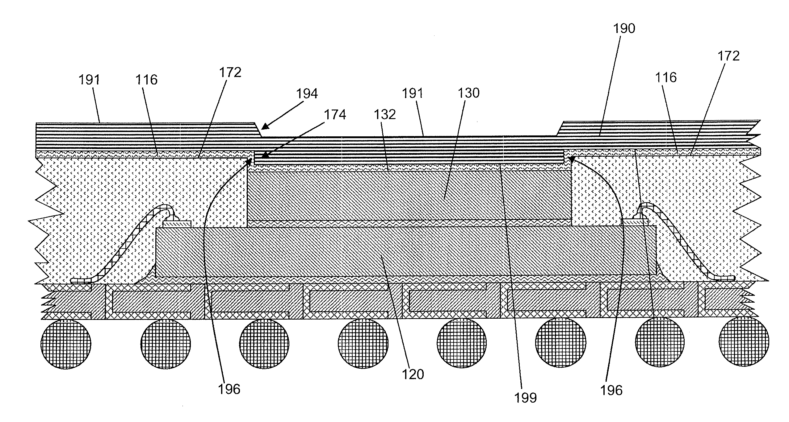
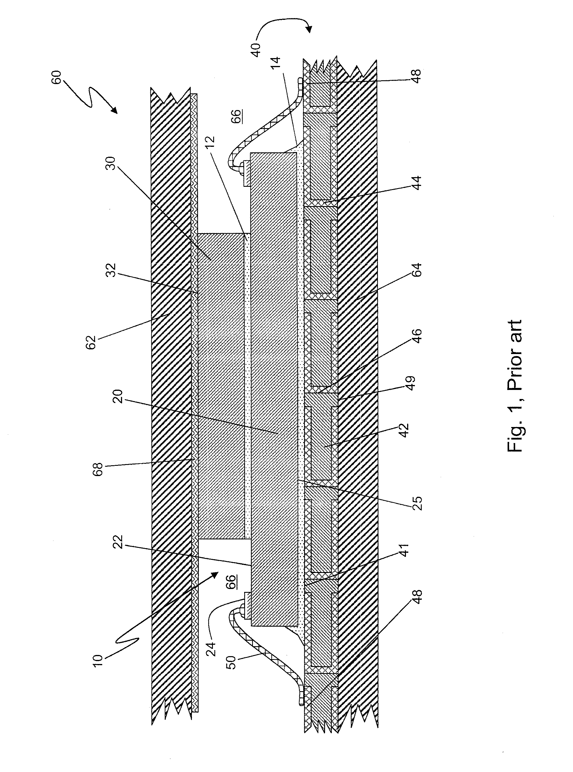
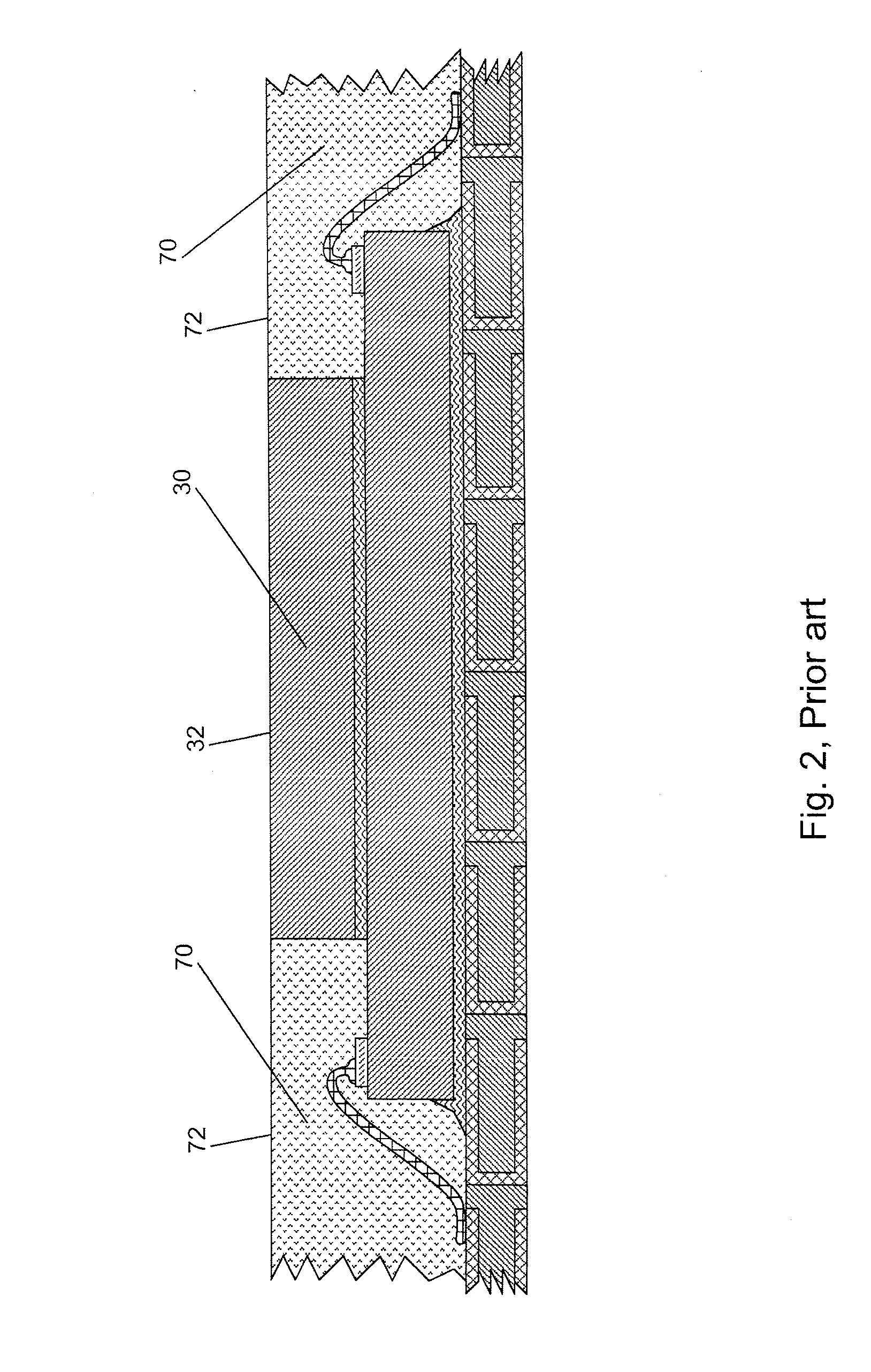
[0032]A packaging method for a circuit die, and related electronic device, is generally described herein, and will be explained with reference to the following non-limiting examples. In the explanations that follow, it should be understood that lists of materials, methods or the like are meant to be inclusive, rather than exclusive, and are intended simply to present indicative sub-sets of potentially much larger sets of related materials, methodologies or the like. Additionally, items shown in the figures are not to scale, but are instead drawn in a manner that simplifies the following description. Additionally, words of orientation such as “top,”“bottom” or the like should not be taken with reference to the preferred orientation of a final product; these words are used merely with reference to the figures for ease of description.

[0033]A flow chart of one embodiment of the instant invention packaging method is shown in FIG. 6. With further reference to FIG. 7, a first embodiment pa...


PUM


Abstract

A circuit die is disposed into a region defined by a mold. A molding material is then introduced into the region to encapsulate the circuit die. Prior to substantial curing of the molding material, at least a portion of the molding material is removed from over a surface of the circuit die, creating a recessed region in the encapsulating material. A heat spreader may then be disposed within the recessed region, as well as over the top surface of the encapsulating material. The heat spreader may have a downset that substantially aligns with the recessed region and reduces the distance between the heat spreader and the spacer for better heat dissipation.

Description

FIELD OF THE INVENTION[0001]The present invention relates generally to the packaging of a circuit die. More particularly, the present invention discloses a method, and related circuit package, that provides a heat spreader disposed over a circuit die with substantially no intervening molding material.BACKGROUND OF THE INVENTION[0002]As circuit dimensions continue to decrease, it has become increasingly important to provide ways to remove heat from the circuit die. Indeed, a significant limiting factor in the speed and density of electronic devices is the ability to satisfactorily remove the heat that such devices develop while operating. To this end, heat spreaders are now commonly employed in many circuit packages.[0003]FIG. 1 illustrates an encapsulation step in the prior art for a Fully Molded and Separated Ball Grid Array (FSBGA). A partially formed FSBGA device 10 includes a circuit die 20, a spacer 30 and a substrate 40 adhered to each other. The circuit die 20 may be any die ...

Claims


Application Information

Patent Timeline
IPC IPC(8): H01L23/36H01L21/56
CPCH01L23/16H01L2224/16225H01L23/36H01L23/4334H01L2224/48091H01L2224/48227H01L2224/48465H01L2224/73265H01L2924/15311H01L2924/10253H01L2224/73253H01L24/48H01L2224/32225H01L2924/1815H01L23/3128H01L2924/00014H01L2924/00012H01L2924/00H01L24/73H01L2924/181H01L2924/00011H01L2224/0401H01L2224/45099H01L2224/45015H01L2924/207H01L23/34H01L21/82
Inventor CHUA, KOK HUANJOMAN, BUDIXIONG, ZHENG PENG
Owner BELL SEMICON LLC
Why Eureka
Try Eureka