Electronic packages

a technology of electronic devices and packaging, applied in the direction of printed circuits, printed circuit stress/warp reduction, dielectric characteristics, etc., can solve the problems the difference in the size of the die, the thickness of the material only augments the difficulty in avoiding assembly deformation, and the possibility of mechanical failure of the combination is still real, so as to achieve greater flexibility in the use of materials and configurations, and the effect of greater range of generated forces

Active Publication Date: 2010-03-02
BELL SEMICON LLC
View PDF2 Cites 2 Cited by
  • Summary
  • Abstract
  • Description
  • Claims
  • Application Information

AI Technical Summary

Benefits of technology

[0010]Thus a greater flexibility in the use of materials and configurations is possible since a greater range of generated forces without failure is tolerated.

Problems solved by technology

Nevertheless, despite these precautions, significant mechanical forces that cause deformation of the assembly are possible.
Additionally, differences in die size, substrate size, bump dimensions, material thicknesses only augment the difficulty in avoiding assembly deformation.
Further, even if the mechanical forces of a die / external body combination are tolerated at one operating temperature, mechanical failure of the combination is still a real possibility due to ambient temperature changes associated with transport or operation.
Mechanical distortion and / or failure, i.e. delamination or cracking at a material layer interface or cohesive failure within a material layer, is a real concern and often is the cause of, or contributing factor to, failure of an electronic component.
Since the materials used in the die / external body assembly are generally dictated by a variety of electrical and mechanical demands associated with other problems there has been little flexibility in expedients used to maintain mechanical stability of the die / external body combination.

Method used


Image

  • Electronic packages
  • Electronic packages
  • Electronic packages

Examples


example

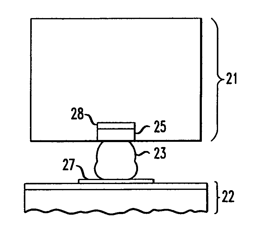
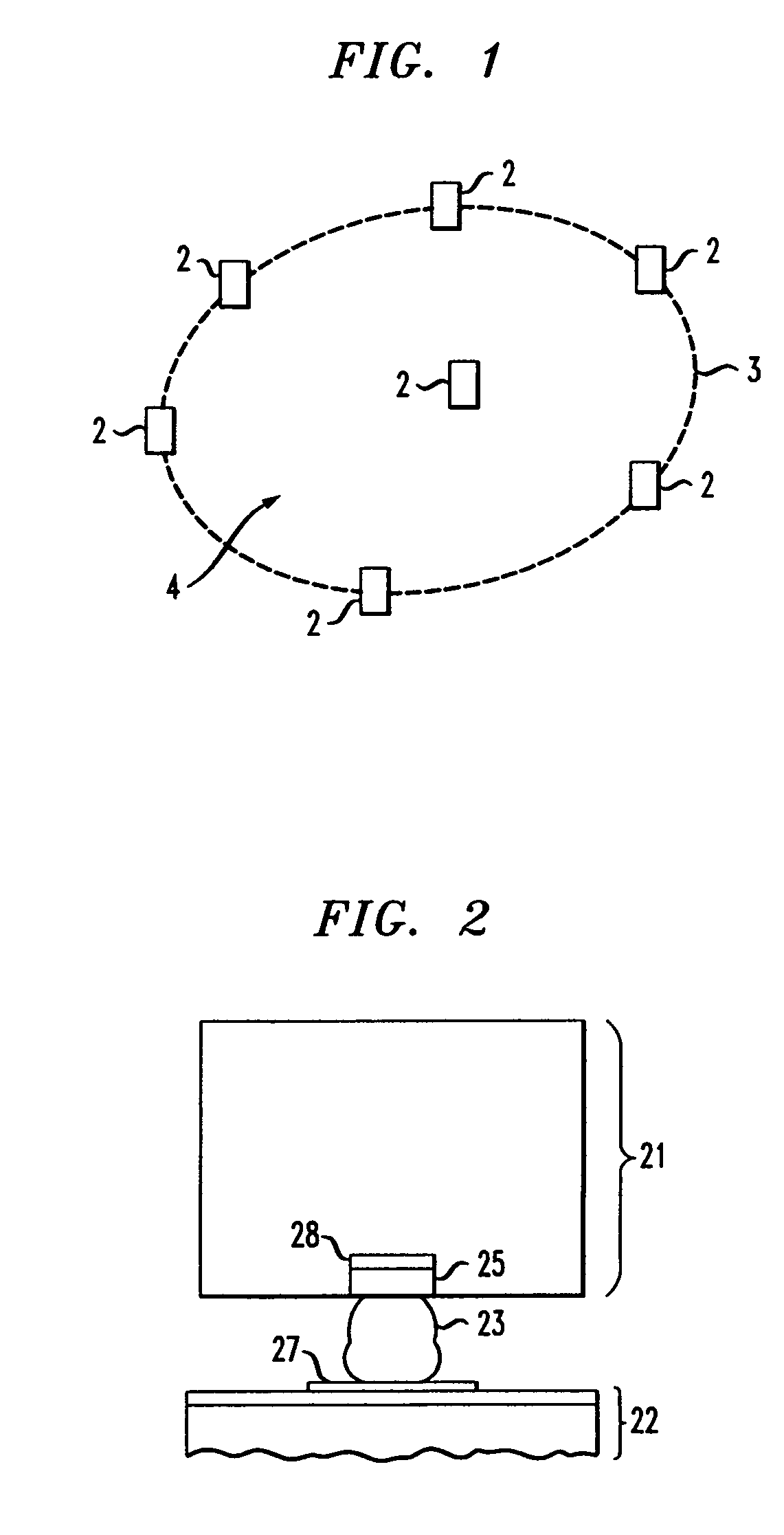
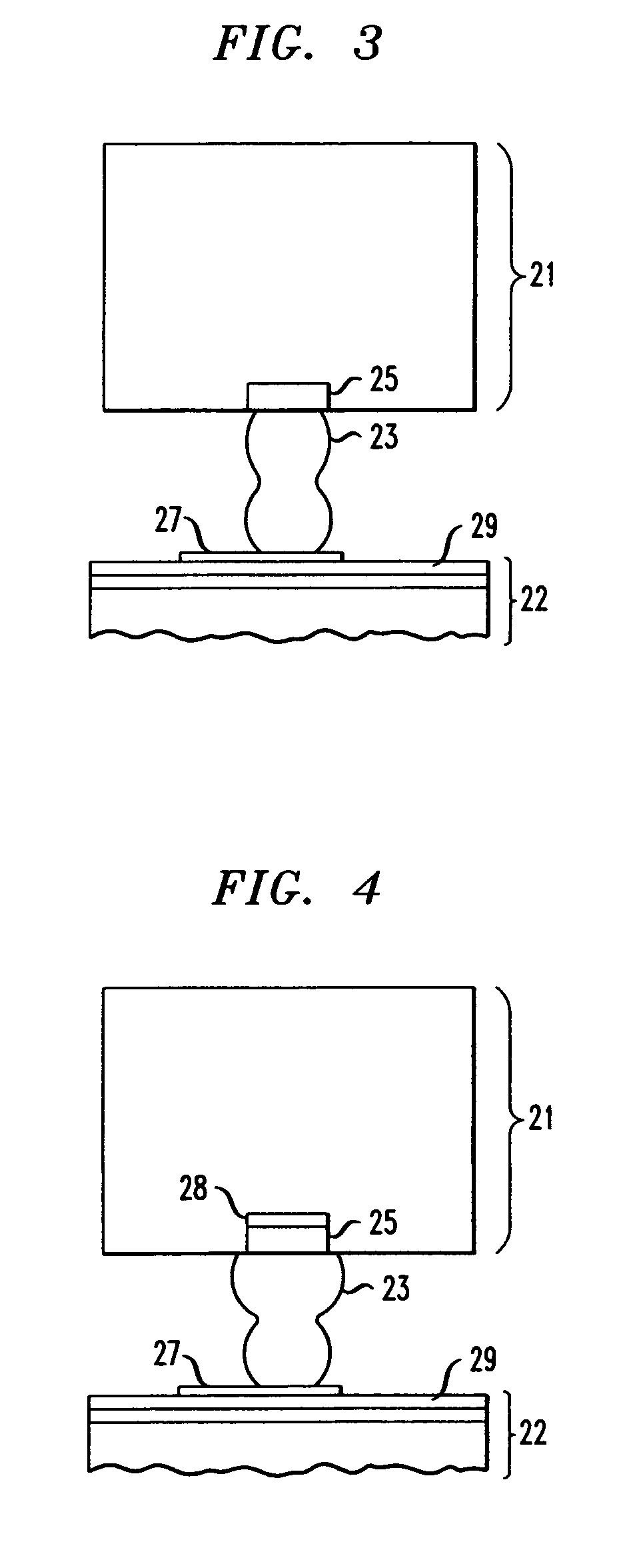
[0022]An assembly of general structure as illustrated in FIG. 3 was fabricated. The assembly included an integrated circuit having bumps in direct contact with a stiff, non-compliant inorganic silicon nitride or silicon oxide layer. The bumps on the silicon integrated circuit were attached to the silicon die of the integrated circuit using standard bump processing including under bump metallization (typically referred to as UBM) that was accomplished by vapor deposition onto the external surface of the die—a surface constituting silicon dioxide and metal circuit pads. The UBM layer is composed of successively deposited layers i.e. 400 nm of vapor deposited aluminum followed by 400 nm of vapor deposited nickel followed by 800 nanometers of copper. (This composite structure acts as the adhesion layer between the die and the solder bump.) The UBM is then patterned using standard photolithography and wet chemical etching. That is, resist material is patterned by lithography to be positi...


PUM


Abstract

Assemblies involving integrated circuit dies (e.g. packaged integrated circuits) and packaged dies electrically connected to circuit boards at times mechanically fail at conducting pads used for electrical interconnection. Such failure is mitigated by underlying appropriate pads with a compliant region having specific characteristics.

Description

TECHNICAL FIELD[0001]This invention relates to electronic devices and in particular packaging of electronic devices such as integrated circuits.BACKGROUND OF THE INVENTION[0002]For integrated circuits i.e., circuits having multiple active elements formed on a silicon substrate, the formation of the circuits on the silicon substrate is only part of the fabrication procedure. The silicon substrate with its subsequent layers added during device formation generally has outermost surface regions—pads—of high electrical conductivity, i.e. conductivity greater than 0.02 (μohm-cm)−1 employed for electrical communication with the integrated circuit. Electrical connection to these pads and the protection of the silicon substrate with its added layers i.e. in totality, the die, is denominated in the trade as packaging.[0003]A variety of methods have been used to connect the die to electronic circuitry external to the die such as by forming an interface between a die package and an external sub...

Claims


Application Information

Patent Timeline
Patent Type & Authority Patents(United States)
IPC IPC(8): H01L31/00
CPCH01L23/49811H01L24/05H05K1/0271H01L24/81H01L2224/04042H01L2924/10253H01L2924/01028H01L2224/48647H01L2224/48624H01L2924/01047H01L2924/01033H01L2924/01006H01L2924/00013H05K2201/10674H05K2201/0133H05K3/3436H01L2924/14H01L2924/014H01L2924/01322H01L2924/01082H01L2924/01079H01L2924/01078H01L2924/0105H01L2924/01029H01L2924/01014H01L24/11H01L24/13H01L24/16H01L2224/0401H01L2224/05624H01L2224/05647H01L2224/1132H01L2224/11849H01L2224/13016H01L2224/131H01L2224/13147H01L2224/16225H01L2224/45144H01L2224/8121H01L2224/81815H01L2924/01013H01L2924/00014H01L2924/01039H01L2224/13099H01L2924/00
Inventor AMIN, AHMED NURBACHMAN, MARK ADAMCROUTHAMEL, DAVID LEEOSENBACH, JOHN WILLIAMVACCARO, BRIAN THOMAS
Owner BELL SEMICON LLC
Why Eureka
Try Eureka