

Method of manufacturing photomask
- Summary
- Abstract
- Description
- Claims
- Application Information
AI Technical Summary
Benefits of technology
Problems solved by technology
Method used
Image

Examples
first preferred embodiment
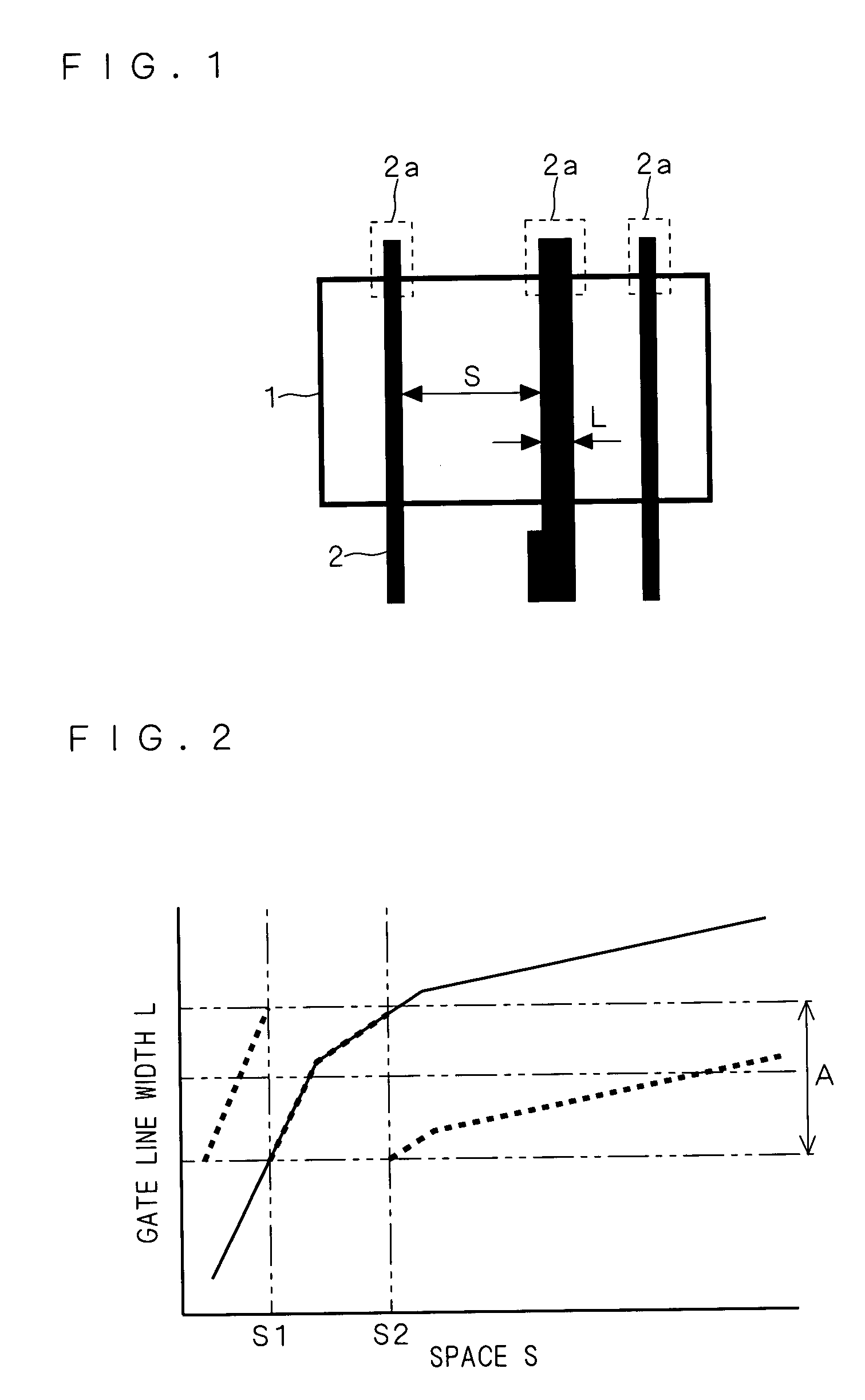
[0022]FIG. 1 is a plan view showing a semiconductor device according to a first preferred embodiment of the invention. As shown, a plurality of gate interconnects 2 are formed on a semiconductor device 1. The gate width of a gate interconnect2 shall be designated as L, and the space between two gate interconnects 2 shall be designated as S. FIG. 2 is a graph plotting finished gate width L against space S. FIG. 2 illustrates by a solid line the gate width L of a gate formed on a substrate in relation to the space S, in which a desired gate width L including manufacturing errors falls within a range indicated by A. Although the gate interconnects 2 are inherently required to be formed with the gate width L falling within the range of A, the optical proximity effect causes the gate width L to be reduced when the space S is narrower than S1.
[0023]On the other hand, when the space S is wider than S2, the optical proximity effect causes the gate width L to be increased. Thus, the optical ...
second preferred embodiment
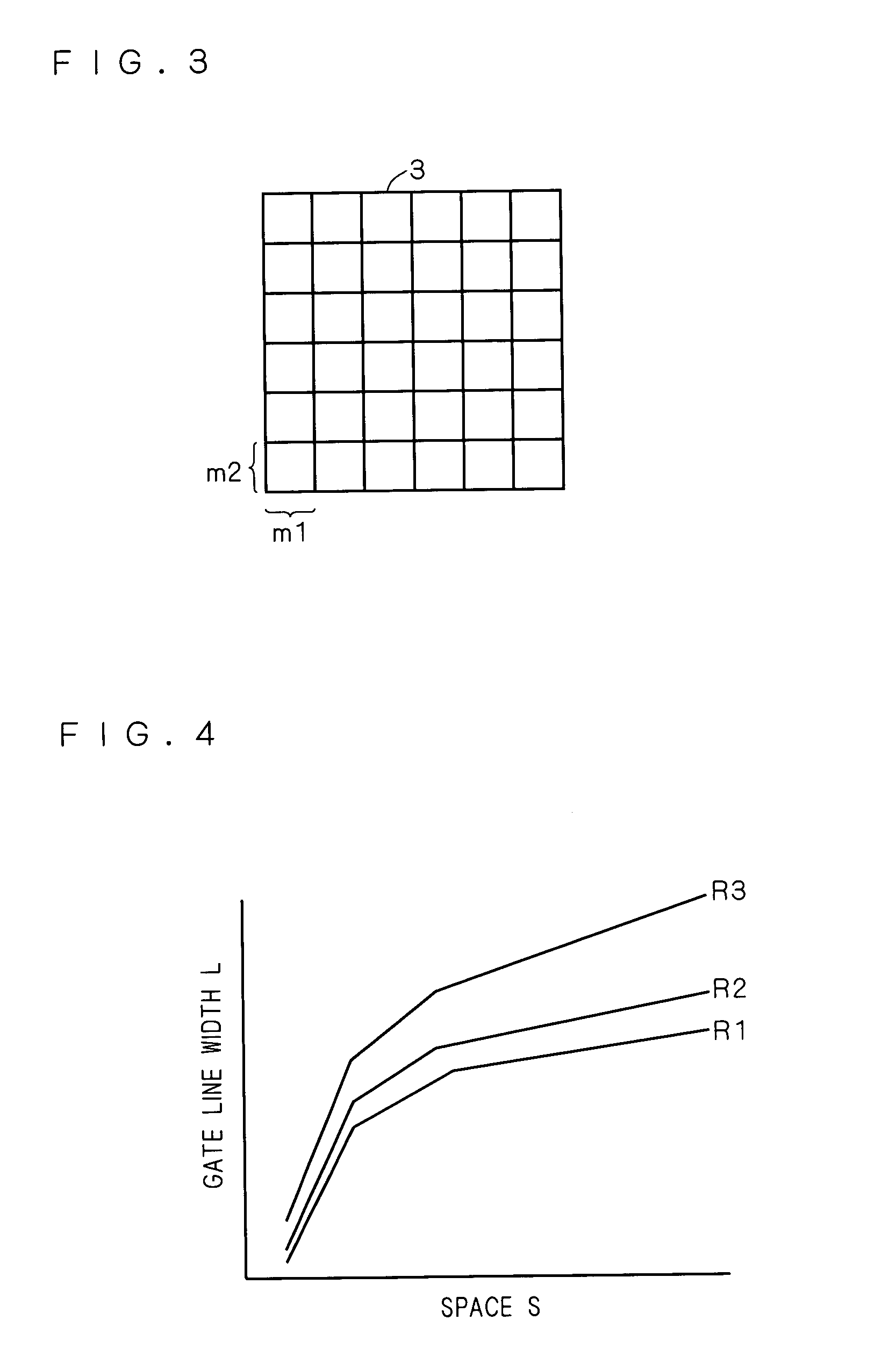
[0033]The present embodiment will also be described taking the size of a photomask as that of a repeating unit of a semiconductor device. As shown in FIG. 3, the photomask 3 is divided into m1×m2 mesh regions M, e.g., 100 μm×100 μm mesh regions M. The occupation rate R of a mask pattern is calculated for each of the mesh regions M. In the present embodiment, description will also be made on the occupation rate R of a gate pattern.
[0034]In the present embodiment, the mask pattern configuration of the photomask 3 is corrected based on the difference in occupation rate R between gate patterns. Thus, the shift of the gate width L with respect to a photomask pattern caused by the pattern density can be corrected. In the present embodiment, a correction table as shown in FIG. 7 is provided such that the amount of correction can be derived from the occupation rate R. Such correction table is obtained through experiments or simulations. For instance, when the occupation rate R of a mesh reg...
third preferred embodiment
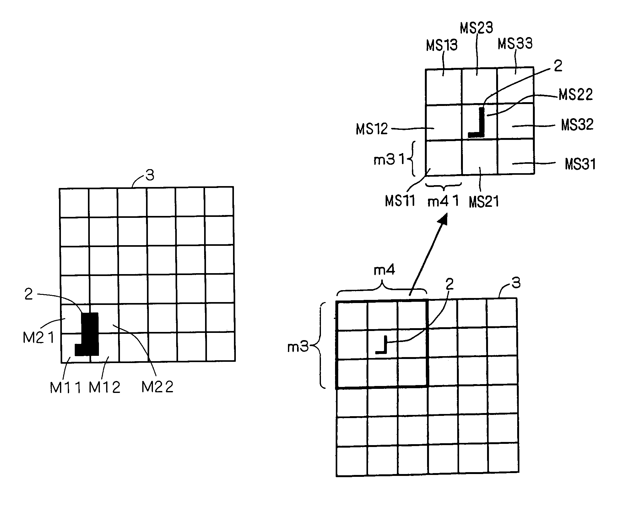
[0040]The present embodiment will also be described taking the size of a photomask as that of a repeating unit of a semiconductor device. FIG. 8 illustrates the photomask 3 divided into m11×m12 mesh regions M. An m11×m12 mesh region M is a region that is affected by factors causing a shift of a finished pattern due to the pattern density in an etching step of a semiconductor device. For instance, the m11×m12 mesh region M is of 100 μm×100 μm size, which is a range where the finished pattern is shifted due to the pattern density when etching polysilicon which serves as the gate interconnects 2. Variations in material, process and the like cause variations in a range where the finished pattern is shifted due to the pattern density which is a correction factor. This requires an optimum size to be selected for a mesh region M for each correction factor.
[0041]The occupation rate R of a mask pattern is calculated for each of m11×m12 mesh regions M. In the present embodiment, description w...
PUM
 Abstract
Description
Claims
Application Information