
Method for programming multi-level cell flash memory device

Active Publication Date: 2009-01-01
SK HYNIX INC
View PDF5 Cites 10 Cited by
  • Summary
  • Abstract
  • Description
  • Claims
  • Application Information

AI Technical Summary

Benefits of technology

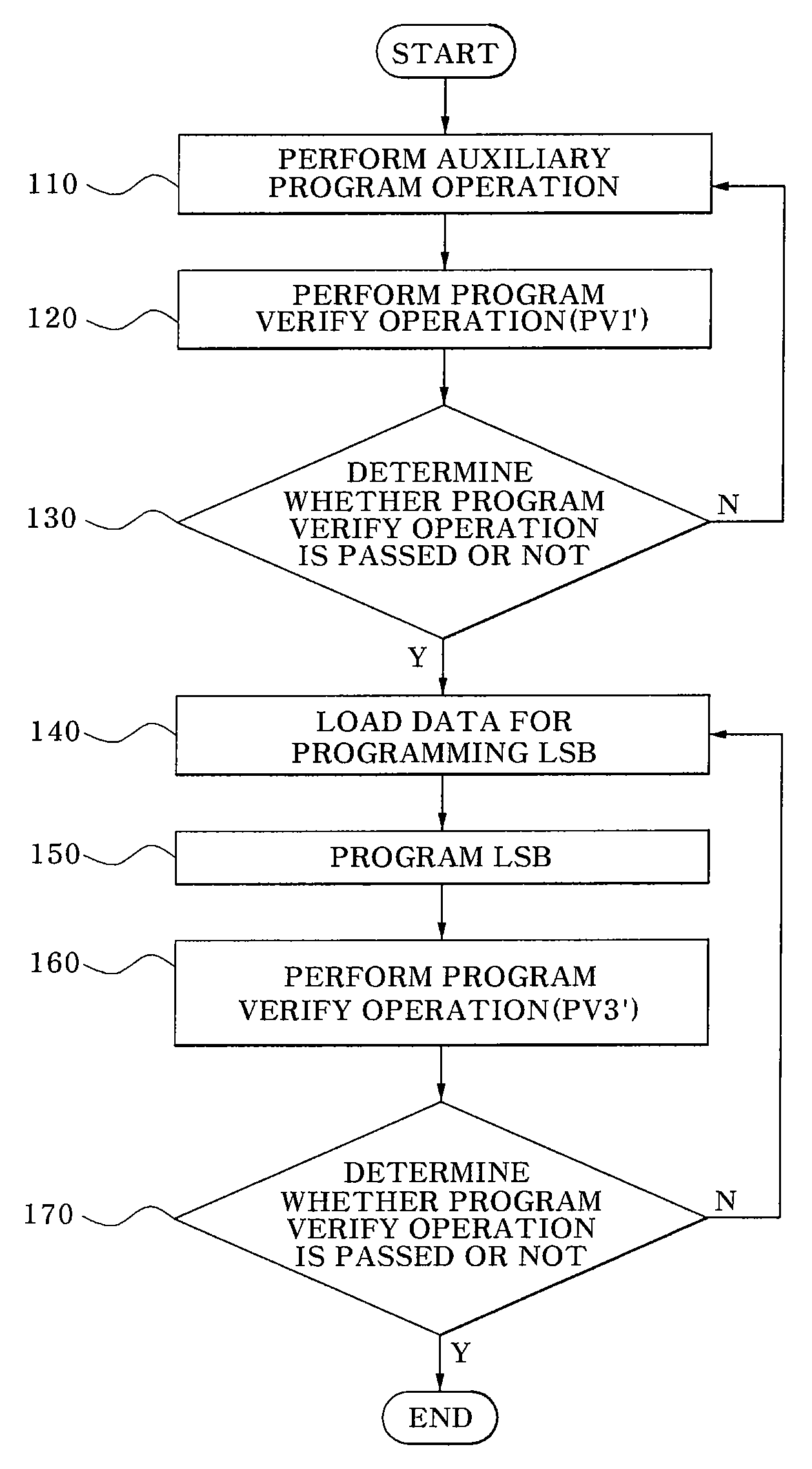
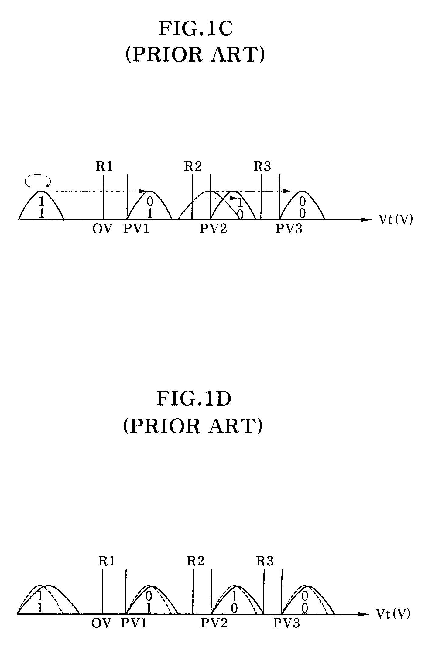
[0015]Embodiments of the present invention are directed to a method for programming an MLC flash memory device to provide a uniform and narrow threshold voltage distribution by minimizing interference of adjacent cells during a program operation of the MLC flash memory device.

Problems solved by technology

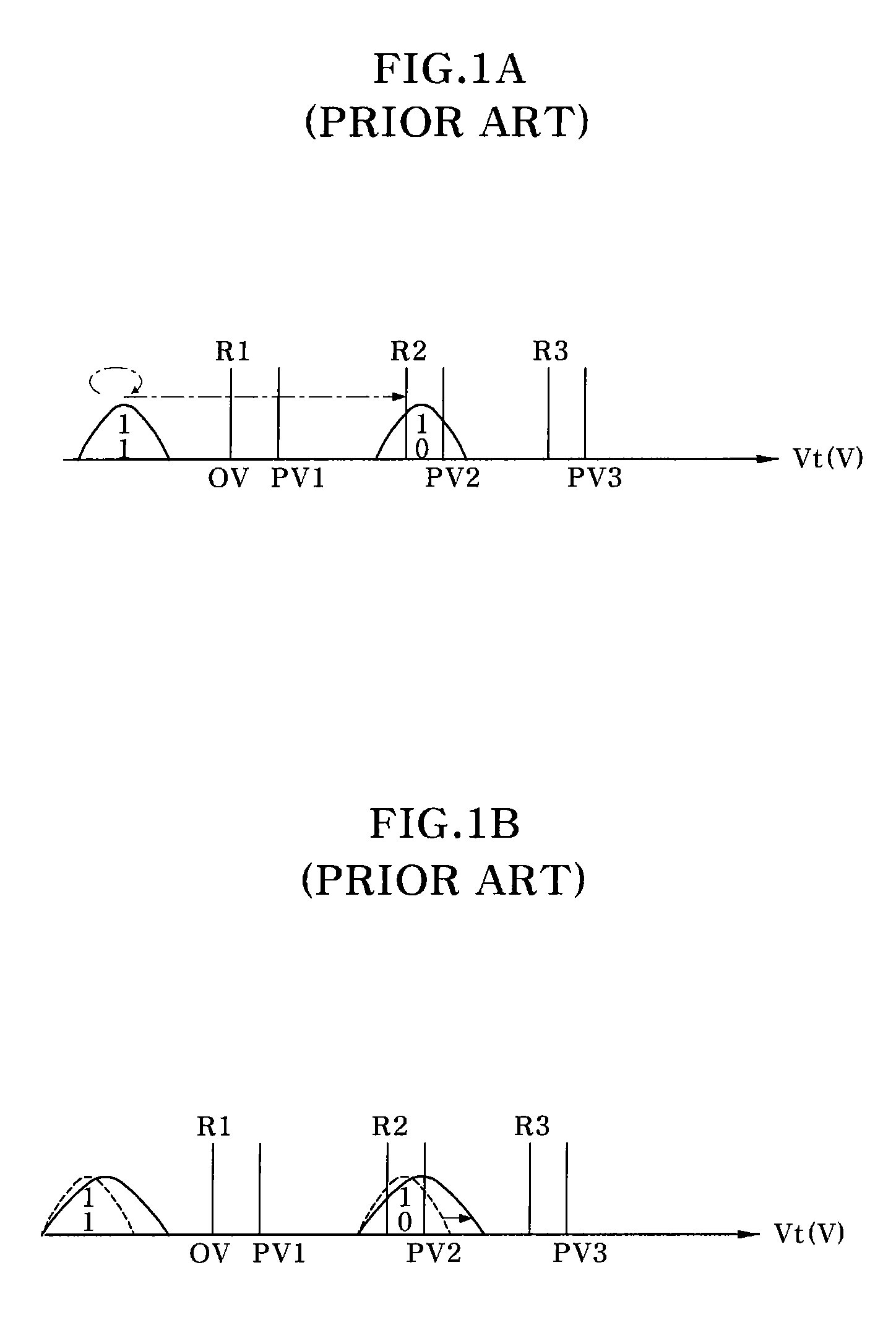
The reason is that it is difficult to accurately measure where a threshold voltage of an actual memory cell is placed in a negative region because a threshold voltage of a memory cell in a [11] state (i.e., an erased state) is negative.
Therefore, failure may easily occur during a read operation.

Method used


Image

  • Method for programming multi-level cell flash memory device
  • Method for programming multi-level cell flash memory device
  • Method for programming multi-level cell flash memory device

Examples


Embodiment Construction

[0027]A method for programming a multi-level cell (MLC) flash memory device in accordance with embodiments of the present invention will be described in detail with reference to the accompanying drawings.

[0028]A program operation of a flash memory device includes injecting electrons to a floating gate of a selected memory cell transistor and verifying whether a threshold voltage of the programmed memory cell transistor reaches a predetermined threshold voltage. The injecting of the electrons and the verifying of the predetermined threshold voltage are repeated on selected memory cells within a predetermined number of program operations until the predetermined threshold voltage is reached.

[0029]To obtain an MLC structure, it is important that the width of threshold voltage distribution in each programmed status is uniform and narrow within predetermined limits. Specifically, a program operation levels a threshold voltage of a memory cell in a [11] state (i.e., an erased state) to abo...


PUM


Abstract

A method for programming an MLC flash memory device minimizes interference between adjacent cells during a program operation, such that threshold voltage distribution becomes narrow and uniform. According to the method, an auxiliary program operation is performed on memory cells to be programmed, such that a majority of the memory cells have a positive threshold voltage. An LSB of a particular memory cell is programmed to a predetermined level, and data of the programmed LSB is sensed. An MSB of the particular memory cell is programmed to a predetermined level according to the sensed data of the LSB.

Description

CROSS-REFERENCE TO RELATED APPLICATIONS[0001]The present application claims priority to Korean patent application number 10-2007-0062954, filed on Jun. 26, 2007, which is incorporated by reference in its entirety.BACKGROUND OF THE INVENTION[0002]The present invention relates to a method for operating a flash memory device, and more particularly, to a method for programming a multi-level cell (MLC) flash memory device.[0003]Flash memory devices are non-volatile memory devices that are programmable and erasable, and are widely used for portable electronics (for example, MP3 players, digital cameras, camcorders, laptop computers, personal digital assistants (PDAs), mobile phones, etc.), computer basic input / output systems (BIOS), printers, USB drivers, etc.[0004]NAND flash memory devices are becoming increasingly popular for use as data storage media. Thus, high capacity flash memory devices are in great demand. Recently, to increase storage capacity in a smaller chip size, research fo...

Claims


Application Information

Patent Timeline
IPC IPC(8): G11C16/06
CPCG11C11/5628G11C2211/5621G11C16/3454G11C16/04G11C16/10G11C16/12G11C16/34
Inventor HWANG, KYUNG PIL
Owner SK HYNIX INC
Learn More