Semiconductor Device with Reduced Capacitance Tolerance Value

Inactive Publication Date: 2009-01-15
INFINEON TECH AG
View PDF8 Cites 17 Cited by
  • Summary
  • Abstract
  • Description
  • Claims
  • Application Information

AI Technical Summary

Benefits of technology

[0007]In one aspect the present invention provides a semiconductor device that includes a functionally significant capacitance, wherein the process-determined

Problems solved by technology

Therefore, in such semiconductor devices, the device function may significantly depend on pr

Method used


Image

  • Semiconductor Device with Reduced Capacitance Tolerance Value
  • Semiconductor Device with Reduced Capacitance Tolerance Value
  • Semiconductor Device with Reduced Capacitance Tolerance Value

Examples


second embodiment

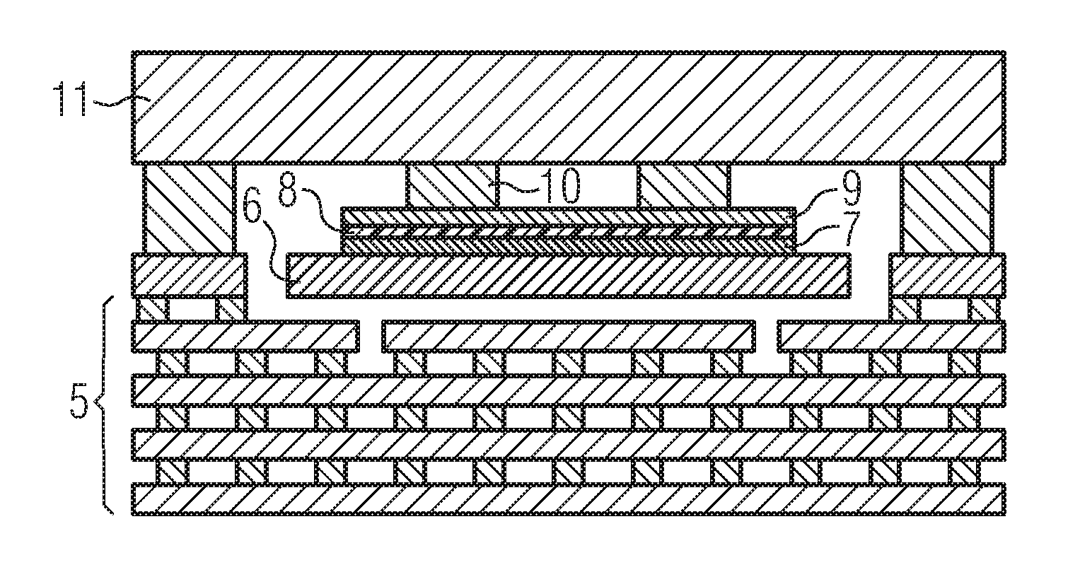
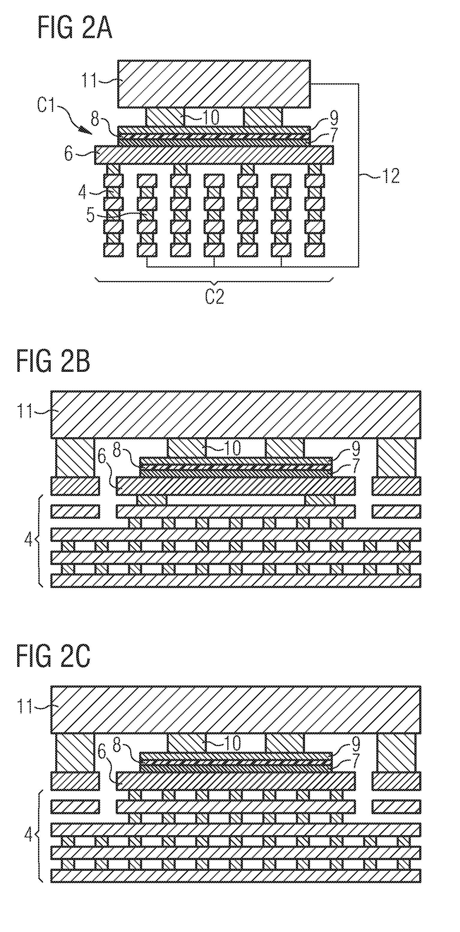
[0029]FIG. 3A schematically shows the layer structure of the invention, in accordance with the schematic circuit diagram of FIG. 3B. This latter figure shows a parallel connection of a first capacitor C1′, a second capacitor C2′, and a third, and fourth capacitor C3.1 and C3.2, together forming an overall capacitance C as a function-determining capacitance C of a semiconductor device (not shown). Deviating from FIGS. 2A to 2E, FIG. 3A shows a surface portion of a semiconductor substrate 13, as well as an MOS structure provided thereon, i.e., a structure formed in a FEOL process, in addition to a BEOL structure provided thereon.

[0030]A P well 14 is provided in the surface of the semiconductor substrate 13, p+ doped regions 15.1, 15.2 are provided with a predetermined distance from each other within the P well 14. On the main surface of the semiconductor substrate 13, bridging the distance between the p+ regions 15.1, 15.2, an oxide layer 16 comprising side wall spacers 16.1, 16.2 is ...

first embodiment

[0033]Like the first embodiment, the formation of the respective capacitor elements, including the sandwich capacitor C2′ and the MOS capacitors C3.1 and C3.2, is basically conventional and, therefore no detailed description in this regard is necessary. However, an adequate connection is essential between the several structures or capacitor elements, respectively, by means of specifically arranged vias, to provide for the intended parallel connection of the various partial capacitances C1′, C2′, C3.1, and C3.2 of the total capacitance C.


PUM


Abstract

A semiconductor device includes a capacitance, the numerical value of which is relevant for a device function. The capacitance is formed from a parallel connection of at least a first and a second capacitor element, wherein the first and second capacitor elements are formed in respective manufacturing steps that exhibit uncorrelated process fluctuations.

Description

TECHNICAL FIELD[0001]The present invention relates to a semiconductor device that includes a capacitance, such as an analog / digital converter device or filter device, a device function of which is significantly influenced by a numerical value of the capacitance.BACKGROUND[0002]The device functions of semiconductor devices are significantly influenced by the numerical value of inherent capacitive elements, which numerical values are influenced by process parameters of respective manufacturing steps of the semiconductor device that result in the formation of those capacitive elements. Therefore, in such semiconductor devices, the device function may significantly depend on process parameter fluctuations that are difficult to control in a sufficiently precise manner.[0003]A first type of capacitor element that may be relevant is a MOS capacitor element originating from the formation of a MOS (metal-oxide-semiconductor) structure in the manufacture of an MOS-type semiconductor element. ...

Claims


Application Information

Patent Timeline
IPC IPC(8): H01L29/94H01L29/00
CPCH01L23/5223H01L27/0688H01L27/0805H01L2924/0002H01L2924/00
Inventor BAUMGARTNER, PETERRIESS, PHILIPPBENETIK, THOMAS
Owner INFINEON TECH AG
Why Eureka
Try Eureka