Thin-film LED (Light-Emitting Diode) device and manufacturing method thereof

An LED device and thin-film technology, applied in semiconductor devices, electrical components, circuits, etc., can solve the problems of complex and precise special equipment for plastic packaging process, broken gold wires on light-guiding panels of devices, high cost of improvement and upgrading, and achieve industrialization. The chemical prospect is considerable, the light-emitting angle is large, and the effect of reducing the use of plastic molding molds and equipment

Active Publication Date: 2013-10-23
SOUTH CHINA UNIV OF TECH
View PDF4 Cites 3 Cited by
  • Summary
  • Abstract
  • Description
  • Claims
  • Application Information

AI Technical Summary

Problems solved by technology

At present, ultra-thin LED TVs have become the mainstream trend, so the demand for ultra-thin LED devices is very urgent. At the same time, no matter whether the direct-type backlight or side-type backlight is used, the device also has the problem of being broken by the light guide panel. golden thread

Method used


Image

  • Thin-film LED (Light-Emitting Diode) device and manufacturing method thereof
  • Thin-film LED (Light-Emitting Diode) device and manufacturing method thereof
  • Thin-film LED (Light-Emitting Diode) device and manufacturing method thereof

Examples


Embodiment 1

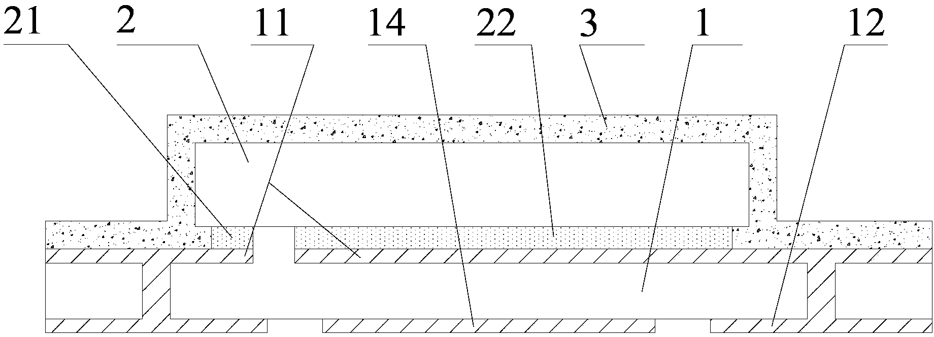
[0036] This embodiment provides a thin-film LED device, which is now combined figure 1 versus figure 2 This invention is specifically described.

[0037] figure 1 Is a structural cross-sectional view of a thin-film LED device according to the present invention, as shown in the figure,

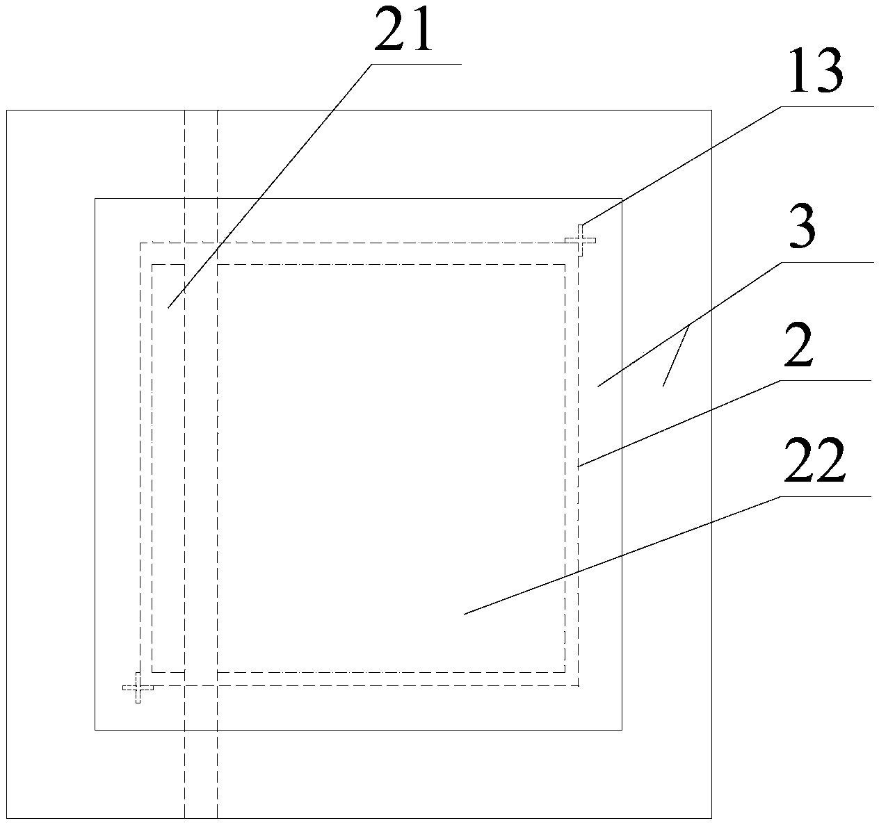
[0038] A thin-film LED device includes a thin-film circuit support 1, an LED chip 2 with a gold wire-free flip-chip structure, and a light-transmitting protective film 3. The LED chip 2 has a thickness of 0.1 mm, and the positive and negative electrodes of the LED chip 2 It is bonded to the upper surface circuit layer 11 of the sheet-type circuit support 1 by eutectic welding, and the lower surface circuit layer 12 of the sheet-type circuit support 1 is connected to the upper surface circuit layer through the circuit and is respectively connected to the positive and negative circuits of the LED chip 2 In connection, the light-transmitting protective film 3 tightly covers the top and surroundings of...

Embodiment 2

[0047] This embodiment proposes a method of manufacturing a thin-film LED device, which is now combined image 3 , Figure 4 versus Figure 5 This is a further description and explanation of the manufacturing method proposed by the present invention.

[0048] A method of manufacturing a thin-film LED device includes the steps:

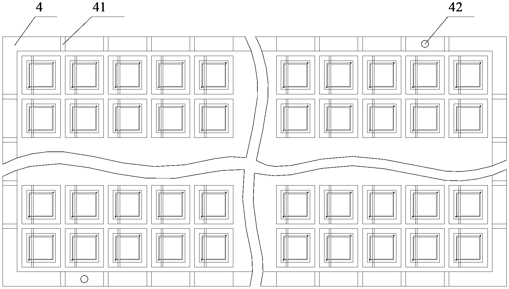
[0049] S1. Flux is placed on the center point of each bracket unit of the sheet-type circuit substrate 4 with positioning holes 42 at the edge, the area of ​​the flux is equivalent to the area of ​​the bottom electrode of the LED chip 2, and the flux is a rosin-like glue;

[0050] S2. Place the LED chip 2 on the sheet-type circuit substrate 4 on which the flux has been spotted. When the LED chip 2 is placed, the LED chip 2 is positioned according to the LED chip placement mark 13;

[0051] S3. Put the sheet-type circuit substrate 4 on which the LED chip 2 is placed into a reflow furnace for eutectic solidification;

[0052] S4. Spray a layer of liquid adhesive 5...

Embodiment 3

[0061] This embodiment proposes a method of manufacturing a thin-film LED device, which is now combined image 3 Figure 4 versus Figure 5 This is a further description and explanation of the manufacturing method proposed by the present invention.

[0062] A method of manufacturing a thin-film LED device includes the steps:

[0063] S1. Flux is placed on the center point of each bracket unit of the sheet-type circuit substrate 4 with positioning holes 42 at the edge, the area of ​​the flux is equivalent to the area of ​​the bottom electrode of the LED chip 2, and the flux is a rosin-like glue;

[0064] S2. Place the LED chip 2 on the sheet-type circuit substrate 4 on which the flux has been spotted. When the LED chip 2 is placed, the LED chip 2 is positioned according to the LED chip placement mark 13;

[0065] S3. Put the sheet-type circuit substrate 4 on which the LED chip 2 is placed into a reflow furnace for eutectic solidification;

[0066] S4. Spray a layer of liquid adhesive 5 u...


PUM

PropertyMeasurementUnit
Thicknessaaaaaaaaaa
Thicknessaaaaaaaaaa
Thicknessaaaaaaaaaa

Abstract

The invention discloses a thin-film LED (Light-Emitting Diode) device and a manufacturing method thereof. The device comprises a sheet circuit substrate, a gold wire-free inverted structure LED chip and a layer of light-passing protective film. The LED chip of the device has an inverted structure, and the electrode of the chip is fixed on the sheet substrate in a eutectic soldering way, so that electrical interconnection free from gold wire bonding is realized; and the layer of light-passing protective film is covered on the surfaces of the chip and the substrate. The electrode of the LED device disclosed by the invention is positioned at the bottom of the device, so that a surface mounting technology can be implemented easily. The device disclosed by the invention is 0.25-0.6 millimeter in thickness, has the advantages of small thickness, small size, large luminous angle, high luminous efficiency, high reliability, simple manufacturing process, high production efficiency, low cost and the like, is suitable for encapsulating high-power and ordinary-power LEDs, and can be widely applied in the fields of illumination, display and the like.

Description

Technical field [0001] The invention relates to a thin film LED device and a manufacturing method thereof, in particular to a structure of an LED device and a preparation method for realizing the structure, and belongs to the field of semiconductor device manufacturing. Background technique [0002] LED light source has become the fourth-generation light source with its high luminous efficiency, energy saving, environmental protection, long life, short response time and many other advantages. It has gradually begun to replace traditional light sources and has shown broad potential in the market. Especially LED light sources are used in huge amounts in the lighting field. Driven by the emergence of emerging application markets, the scale of the LED market has increased rapidly in recent years. The market demand for LEDs has risen sharply, especially for devices that are small in size, large in light-emitting area, and thin. In lighting products, many LED devices have reached the...

Claims


Application Information

Patent Timeline
IPC IPC(8): H01L33/48H01L33/52
CPCH01L33/50H01L33/0095H01L33/56H01L2933/0041H01L2933/0091
Inventor 汤勇余彬海李宗涛丁鑫锐陆龙生袁伟万珍平
Owner SOUTH CHINA UNIV OF TECH
Why Eureka
Try Eureka