Unlock instant, AI-driven research and patent intelligence for your innovation.

Methods of reading data from non-volatile semiconductor memory device

a non-volatile, semiconductor technology, applied in the direction of static storage, digital storage, instruments, etc., can solve the problems of rc delay, coupling noise and/or disturban

Active Publication Date: 2009-01-15
SAMSUNG ELECTRONICS CO LTD
View PDF1 Cites 17 Cited by
  • Summary
  • Abstract
  • Description
  • Claims
  • Application Information

AI Technical Summary

Benefits of technology

[0014]According to one aspect of the present invention, there is provided a method of reading data in a non-volatile memory device. The method includes applying a bit line read voltage to a bit line electrically connected to a selected cell located in a selected string and applying a selected cell read voltage to a word line electrically connected to the selected cell. A first read voltage is applied to word lines electrically connected to first non-selected cells in the selected string and the first non-selected cells are separated from the selected cell. A second read voltage is applied to word lines electrically connected to second non-selected cells in the selected string and the second non-selected cells are adjacent to the selected cell. The second read voltage inhibits a fringe field affecting a thr

Problems solved by technology

This generates RC delay, coupling noise and / or disturbance between adjacent word lines, for example.

Method used


Image

  • Methods of reading data from non-volatile semiconductor memory device
  • Methods of reading data from non-volatile semiconductor memory device
  • Methods of reading data from non-volatile semiconductor memory device

Examples


experiment 1

[0087

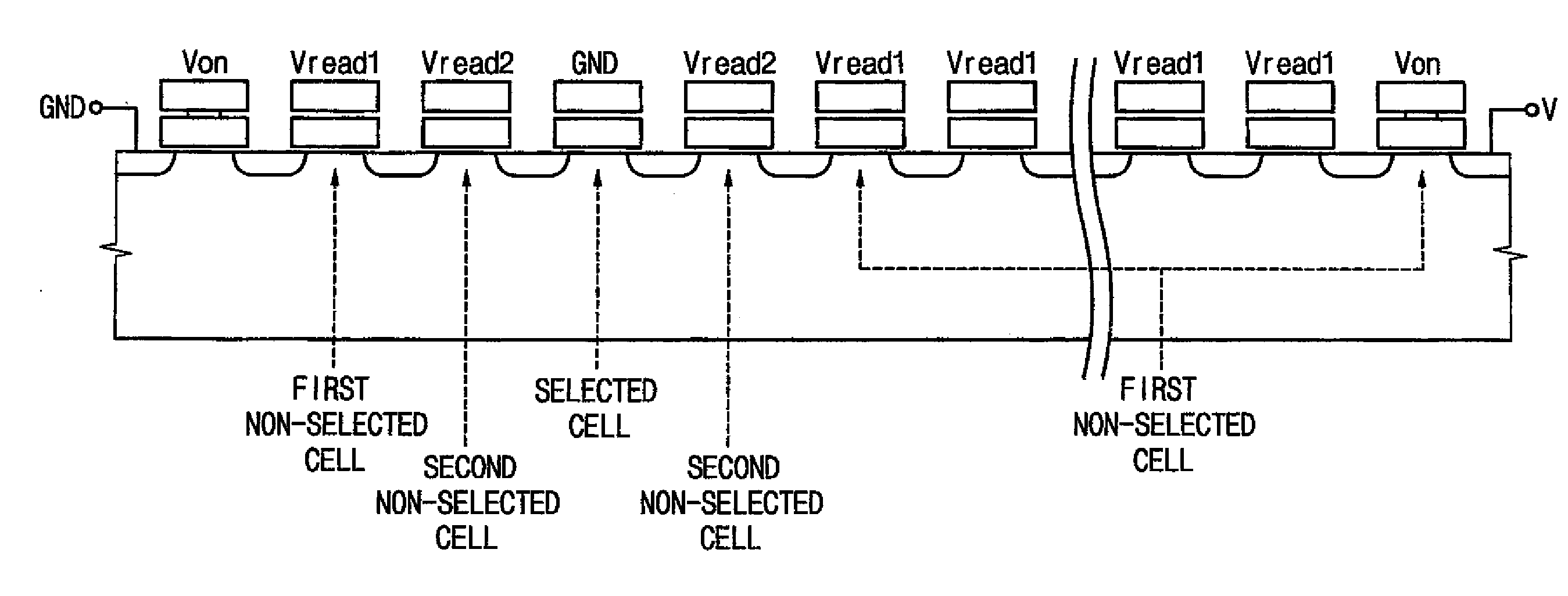
[0088]Voltages were applied to word lines in a NAND type flash memory device, and then threshold voltages were measured in selected cells. In the NAND type flash memory device, a first read voltage was applied to word lines electrically connected to first non-selected cells not adjacent to the selected cell. A second read voltage was applied to word lines electrically connected to second non-selected cells adjacent to the selected cell. A maximum threshold voltage of the memory cells in which data were programmed was about 4.2V.

[0089]While the first read voltage of about 5.5V was applied to the word lines electrically connected to the first non-selected cells, the second read voltages of about 4.6V, about 5.0V and about 5.5V were applied to the word lines electrically connected to the second non-selected cells, respectively. The threshold voltages of the selected cells were measured, respectively. The results are illustrated in FIG. 8.

[0090]Referring to FIG. 8, with the first r...

experiment 2

[0091

[0092]Voltages were applied to word lines in a NAND type flash memory device through substantially the same method discussed above with respect to Example 1, except for the values of first and second read voltages applied to word lines electrically connected to first and second non-selected cells, respectively. While a second read voltage of about 4.6V was applied to the word lines electrically connected to the second non-selected cells, first read voltages of about 4.6V, about 5.0V and about 5.5V were applied to the word lines electrically connected to the first non-selected cells. The threshold voltages were measured in the selected cells, respectively. The results are shown in FIG. 9.

[0093]Referring to FIG. 9, when the second read voltage of about 4.6V, which is substantially higher than the maximum threshold voltage by about 0.4V, was applied to the word lines electrically connected to the second non-selected cells, the threshold voltage of the selected cell did not change ...


PUM


Abstract

A method of reading data in a non-volatile memory device includes applying a bit line read voltage to a bit line and a selected cell read voltage to a word line, both of which are electrically connected to a selected cell located in a selected string. A first read voltage is applied to word lines electrically connected to first non-selected cells separated from the selected cell in the selected string, and a second read voltage is applied to word lines electrically connected to second non-selected cells adjacent to the selected cell in the selected string. The second read voltage is lower than the first read voltage. A pass voltage is applied to turn on a string select transistor and a ground select transistor, respectively, in the selected string. An electrical signal output from the selected string is compared with a standard signal to read data stored in the selected cell.

Description

CROSS-REFERENCE TO RELATED PATENT APPLICATION[0001]A claim of priority is made to Korean Patent Application No. 10-2007-0068940, filed on Jul. 10, 2007, the subject matter of which is hereby incorporated by reference.BACKGROUND OF THE INVENTION[0002]1. Field of the Invention[0003]Example embodiments of the present invention relate to a method of reading data from semiconductor memory devices. More particularly, example embodiments of the present invention relate to reading data in non-volatile semiconductor memory devices using different read voltages.[0004]2. Description of the Related Art[0005]A flash memory device is one type of non-volatile semiconductor memory device, which continuously maintains stored data. Data may be electronically programmed in or erased from flash memory devices. Further, flash memory devices may not require refresh operations. A flash memory device may be classified according to its structure as a NAND type flash memory device and a NOR type flash memory...

Claims


Application Information

Patent Timeline
IPC IPC(8): G11C16/06G11C7/00
CPCG11C16/0483G11C16/3418G11C16/26G11C16/02G11C16/30G11C16/34
Inventor CHOI, BYUNG-YONGFAYRUSHIN, ALBERT
Owner SAMSUNG ELECTRONICS CO LTD