Supercharge Your Innovation With Domain-Expert AI Agents!

Solder bump forming method

a technology of forming method and soldering, which is applied in the direction of soldering apparatus, semiconductor/solid-state device details, manufacturing tools, etc., can solve the problems of increasing the manufacturing cost of the substrate b>10/b>, the proximity of solder balls, etc., and achieves the effect of reliably mounting a conductive ball and reducing a manufacturing cos

Active Publication Date: 2009-01-22
SHINKO ELECTRIC IND CO LTD
View PDF6 Cites 3 Cited by
  • Summary
  • Abstract
  • Description
  • Claims
  • Application Information

AI Technical Summary

Benefits of technology

The present invention provides a method for forming solder bumps on pads with reduced manufacturing costs and improved reliability. The method involves a metal film forming step of chemically reacting a tackifying compound with the pads, an organic sticking layer forming step of chemically reacting the metal film with a solution containing the tackifying compound, and a conductive ball mounting step of supplying the conductive ball on the organic sticking layer, through the metal film and onto the pads. This method eliminates the need for a conductive ball mounting mask, reducing manufacturing costs. Additionally, a diffusion preventing film may be used to prevent copper from diffusing into the solder bump. Overall, this method improves the accuracy and reliability of mounting conductive balls on pads.

Problems solved by technology

However, in the process for forming the flux in FIG. 37, there is a problem in that a relative misalignment of the opening portion 23B of the flux forming mask 23A and the opening portion 17A of the solder resist 17 is generated and the flux which is not applied to the bump forming region 16A or the flux which is applied on the surface of the solder resist 17 is formed.
Further, there is a problem in that the conductive ball 28 is mounted on parts other than the pad 16, and then it is melt and flow out at reflow treatment, thereby causing a problem such as a short between the adjacent solder balls.
Therefore, there is a problem in that a part of the flux is adhered to the surface of the solder resist 17 and an area where the flux is applied becomes large, and thus, there is a possibility that the plurality of conductive balls is mounted on one pad.
Moreover, the related-art solder bump forming method has a problem in that a manufacturing cost of the substrate 10 is increased because the conductive ball mounting mask 26 is used.

Method used


Image

  • Solder bump forming method
  • Solder bump forming method
  • Solder bump forming method

Examples


first embodiment

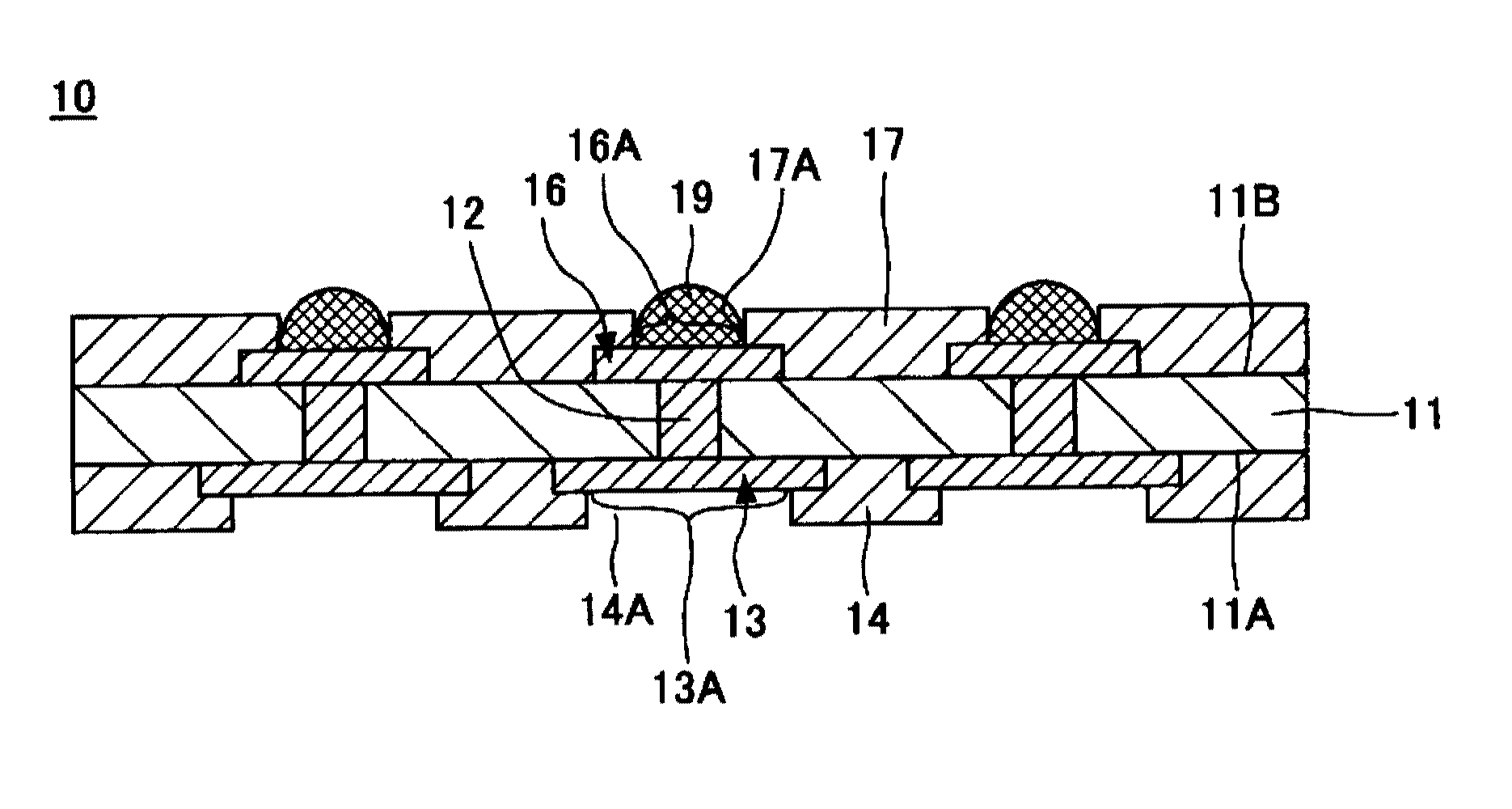
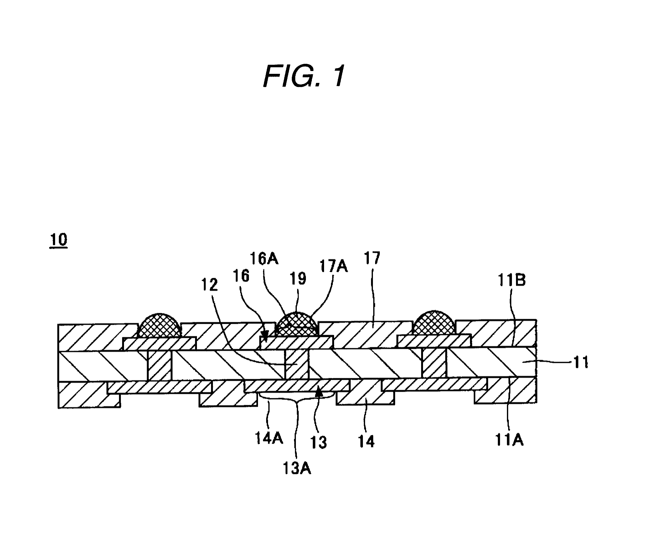
[0073]FIG. 9 is a sectional view showing a substrate according to a first embodiment of the invention.

[0074]With reference to FIG. 9, a substrate 100 according to the embodiment has a substrate body 101, a through electrode 102, a plurality of pads 103 and 107, solder resists 104 and 108, diffusion preventing films 105 and 109, a metal film 111, and a solder bump 112. In the embodiment, the following description will be given by taking, as an example of the substrate 100, a wiring board to be used as a semiconductor package.

[0075]The substrate body 101 takes a shape of a plate and has a plurality of through holes 115. The through electrode 102 is provided in the through holes 115. A lower end of the through electrode 102 is connected to the pad 103 and an upper end of the through electrode 102 is connected to the pad 107. The through electrode 102 serves to electrically connect the pad 103 to the pad 107. For the through electrode 102, it is possible to use a Cu plated film formed b...

second embodiment

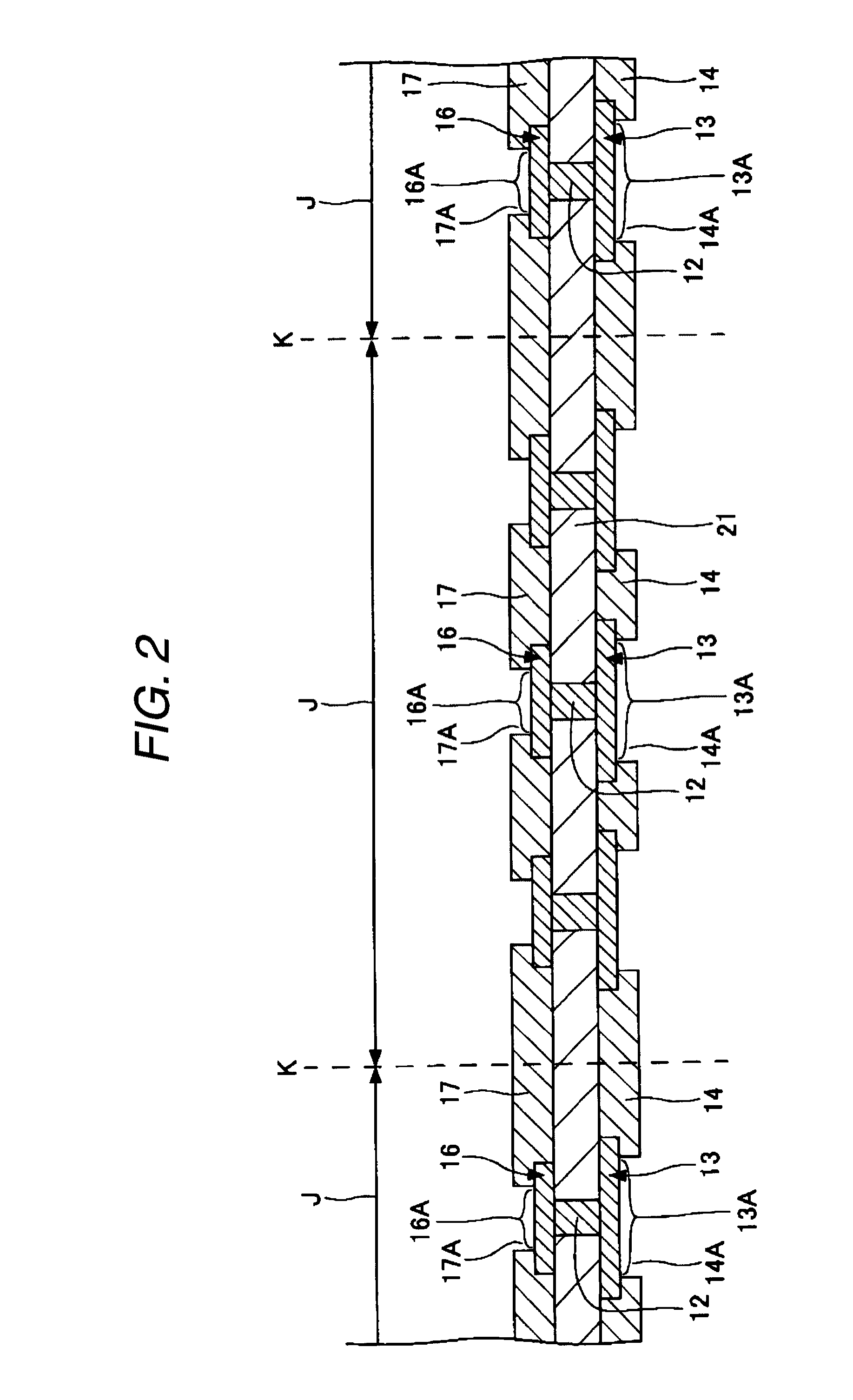
[0124]FIG. 24 is a sectional view showing a substrate according to a second embodiment of the invention. In FIG. 24, the same components as those in the substrate 100 according to the first embodiment have the same reference numerals.

[0125]With reference to FIG. 24, a substrate 150 according to the second embodiment has the same structure as that of the substrate 100 except that a metal film 151 is provided in place of the diffusion preventing film 109 and the metal film 111 which are provided in the substrate 100 according to the first embodiment.

[0126]The metal film 151 is provided to cover a surface 121A of a connecting portion 121 an opposite side to a surface provided in contact with an upper surface 101B of the substrate body 101. The metal film 151 can chemically react to the tackifying compound described in the first embodiment. The metal film 151 serves to react to a solution containing the tackifying compound described in the first embodiment, thereby forming an organic st...


PUM

PropertyMeasurementUnit
thicknessaaaaaaaaaa
diameter R1aaaaaaaaaa
diameter R2aaaaaaaaaa

Abstract

A solder bump forming method of carrying out a reflow treatment over a conductive ball mounted on a plurality of pads, thereby forming a solder bump, includes a metal film forming step of forming a metal film capable of chemically reacting to a tackifying compound on the pads, an organic sticking layer forming step of causing a solution containing the tackifying compound to chemically react to the metal film, thereby forming an organic sticking layer on the metal film, and a conductive ball mounting step of supplying the conductive ball on the pads having the organic sticking layer formed thereon, thereby mounting the conductive ball on the pads through the metal film.

Description

TECHNICAL FIELD[0001]The present invention relates to a solder bump forming method and more particularly to a solder bump forming method of mounting a conductive ball on each of a plurality of pads provided on a wiring board, a package such as a chip size package or a substrate such as a semiconductor chip, thereby forming the solder bump.RELATED ART [0002]FIG. 1 is a sectional view showing a related-art substrate.[0003]With reference to FIG. 1, a related-art substrate 10 has a substrate body 11, a through electrode 12, a plurality of pads 13 and 16, solder resists 14 and 17, and a solder bump 19. The following description will be given by taking, as an example of the substrate 10, a wiring board to be used as a semiconductor package.[0004]The through electrode 12 is provided to penetrate the substrate body 11. A lower end of the through electrode 12 is connected to the pad 13 and an upper end of the through electrode 12 is connected to the pad 16. The through electrode 12 serves to...

Claims


Application Information

Patent Timeline
Patent Type & Authority Applications(United States)
IPC IPC(8): H01L21/768
CPCB23K1/0016H01L2924/01019B23K2201/42H01L21/4853H01L23/481H01L2224/16H01L2924/01046H01L2924/01078H01L2924/01079H05K3/244H05K3/3478H05K2203/041H05K2203/043H05K2203/124B23K3/0623B23K2101/42
Inventor IMAFUJI, KEINAKAZAWA, MASAOSANADA, MASAKIODA, SACHIKOKODAIRA, TADASHINAGATA, KINJIYAMAZAKI, MASARUENOKI, KENJIRO
Owner SHINKO ELECTRIC IND CO LTD
Features
  • R&D
  • Intellectual Property
  • Life Sciences
  • Materials
  • Tech Scout
  • Unparalleled Data Quality
  • Higher Quality Content
  • 60% Fewer Hallucinations
Learn More