Memory module capable of lessening shock stress

a memory module and shock stress technology, applied in the field of memory modules, can solve the problems of existing memory modules that cannot stand impact stress, memory modules that will accidentally drop to the ground, and existing memory modules b>100/b> cannot stand, so as to reduce impact stress

Inactive Publication Date: 2009-01-29
POWERTECH TECHNOLOGY
View PDF7 Cites 8 Cited by
  • Summary
  • Abstract
  • Description
  • Claims
  • Application Information

AI Technical Summary

Benefits of technology

[0005]The main purpose of the present invention is to provide a memory module capable of lessening shock stresses by using stress-buffering layers disposed on the edges of the multi-layer printed circuit board to reduce the impact stresses exerted on the memory module to prevent electrical open caused by dropping.
[0006]The second purpose of the present invention is to provide a memory module capable of lessening shock stresses by using stress-buffering layers to prevent moisture diffusion from the sidewalls of the multi-layer printed circuit board to enhance anti-humidity and product reliability.
[0007]According to the present invention, a memory module primarily comprises a multi-layer printed circuit board (PCB), a plurality of memory packages, and a stress-buffering layer. The PCB has a rectangular first surface, a rectangular second surface, a first long side, a second long side, and two short sides where a plurality of gold fingers are disposed on both surfaces of the first long side and at least a locking slot disposed on each short side. The memory packages are at least disposed on the first surface of the PCB and the stress-buffering layers are formed on two short sides and extended to the first surface and the second surface. A plurality of ball pads are disposed on the first surface of the PCB for joining the solder balls where the ball pads are Non-Solder Mask Defined Pad (NSMD) in one embodiment. The stress-buffering layer can prevent moisture diffusing into the PCB. Moreover, the stress-buffering can further be installed at the second long side. Parts of the memory packages may be also disposed on the second surface of the PCB.

Problems solved by technology

During shipping, handling, and replacement, sometimes memory modules will accidentally drop to the ground.
The existing memory modules can not stand the impact stresses and suffer damaged leading to electrical open.
However, the existing memory module 100 can not stand the impact stresses leading to electrical open and fail the drop test.
The memory module 100 is damaged and failed.

Method used


Image

  • Memory module capable of lessening shock stress
  • Memory module capable of lessening shock stress
  • Memory module capable of lessening shock stress

Examples


first embodiment

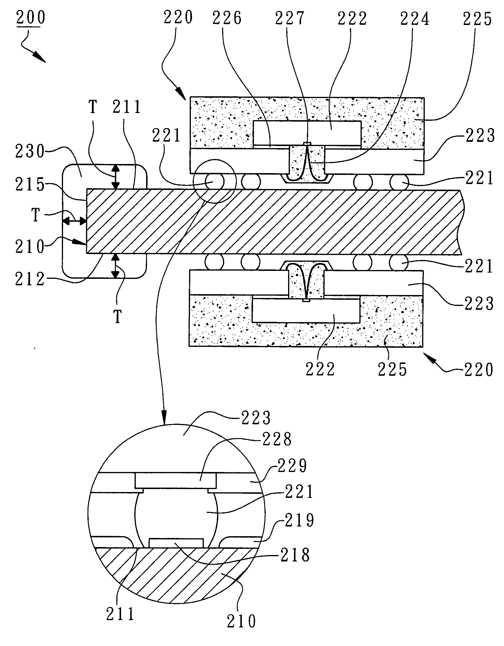
[0016]According to the present invention, as shown in FIG. 4, FIG. 5, and FIG. 6, a memory module 200 primarily comprises a multi-layer printed circuit board (PCB) 210, a plurality of memory packages 220, and a stress-buffering layer 230. The memory module 200 further comprises a plurality of passive components, not shown in the figure, disposed on the PCB 210.

[0017]As shown in FIG. 4 and FIG. 5, the PCB 210 has a rectangular first surface 211, a rectangular second surface 212, a first long side 213, a second long side 214, and two short sides 215 where a plurality of gold fingers 216 are disposed on both surfaces of the first long side 213, i.e., on the same sides of the first surface 211 and the second surface 212 for plugging into the sockets of a desk top computer or a notebook computer, not shown in the figure. Moreover, at least a locking slot 217 is formed on each short side 215 where the locking slots 217 are used to fix the memory module 200 on a mother board by locking dev...

second embodiment

[0022]In the second embodiment, another memory module capable of lessening shock stresses is revealed for desktop computers such as DDR II-400, DDR II-533, DDR II-667, DDR II-800, or DDR III memory modules.

[0023]As shown in FIG. 7, a memory module 300 primarily comprises a PCB 310, a plurality of memory packages 320, and a stress-buffering layer 330. The PCB 310 has a rectangular first surface 311, a rectangular second surface opposing to the first surface 311, a first long side 313, a second long side 314, and two short sides 315 where a plurality of gold fingers 316 are disposed on both surfaces of the first long side 313. The memory packages 320 are at least disposed on one of the surface of the PCB 310, i.e., on the first surface 311 or / and on the second surface.

[0024]The stress-buffering layer 330 is at least disposed on both short sides 315 of the PCB 310 and extended to the first surface 311 and the second surface, not shown in the figure. The Young's modulus of the stress-bu...


PUM


Abstract

A memory module capable of lessening shock stresses, primarily comprises a multi-layer printed circuit board (PCB), a plurality of memory packages, and a stress-buffering layer. The memory packages are disposed at least on one of the rectangular surfaces of the PCB. The stress-buffering layer is disposed at least on both short sides of the PCB and extended to the two rectangular surfaces to reduce the impact stresses. Preferably, the stress-buffering layer is further disposed on the other long side of the PCB opposite to the one with disposed gold fingers.

Description

FIELD OF THE INVENTION[0001]The present invention relates to a memory module for computer systems, especially, to a memory module capable of lessening shock stresses.BACKGROUND OF THE INVENTION[0002]Memory modules are key components in desktop computers or notebook computers where memory modules can repeatedly plug into the sockets on a mother board for operations and calculations of the computer systems. The existing memory modules include SIMM (Single In-Line Memory Module), DIMM (Dual In-Line Memory Module), and SO-DIMM (Small Outline Dual In-Line Memory Module). During shipping, handling, and replacement, sometimes memory modules will accidentally drop to the ground. The existing memory modules can not stand the impact stresses and suffer damaged leading to electrical open.[0003]As shown in FIG. 1, a conventional memory module 100 includes a multi-layer printed circuit board 110 and a plurality of memory packages 120 where the multi-layer printed circuit board 110 has two long s...

Claims


Application Information

Patent Timeline
Patent Type & Authority Applications(United States)
IPC IPC(8): H01L23/02
CPCH05K1/0271H05K1/181H05K2201/09145H05K2203/1572H05K2201/10734H05K2201/2009H05K2201/10159H01L2224/32225H01L2224/4824H01L2224/73215H01L2924/15311H01L2924/00
Inventor FAN, WEN-JENG
Owner POWERTECH TECHNOLOGY
Why Eureka
Try Eureka