Method of fabricating a 3-D device and device made thereby

a three-dimensional device and device technology, applied in the direction of semiconductor devices, semiconductor/solid-state device details, electrical devices, etc., can solve the problem that existing packages, however, may not meet all of the above-described requirements for next-generation devices

Active Publication Date: 2009-02-05
SAMSUNG ELECTRONICS CO LTD
View PDF7 Cites 127 Cited by
  • Summary
  • Abstract
  • Description
  • Claims
  • Application Information

AI Technical Summary

Problems solved by technology

Existing packages, however, may not fulfill all of the above-described requirements for next-generation devices.

Method used


Image

  • Method of fabricating a 3-D device and device made thereby
  • Method of fabricating a 3-D device and device made thereby
  • Method of fabricating a 3-D device and device made thereby

Examples


first embodiment

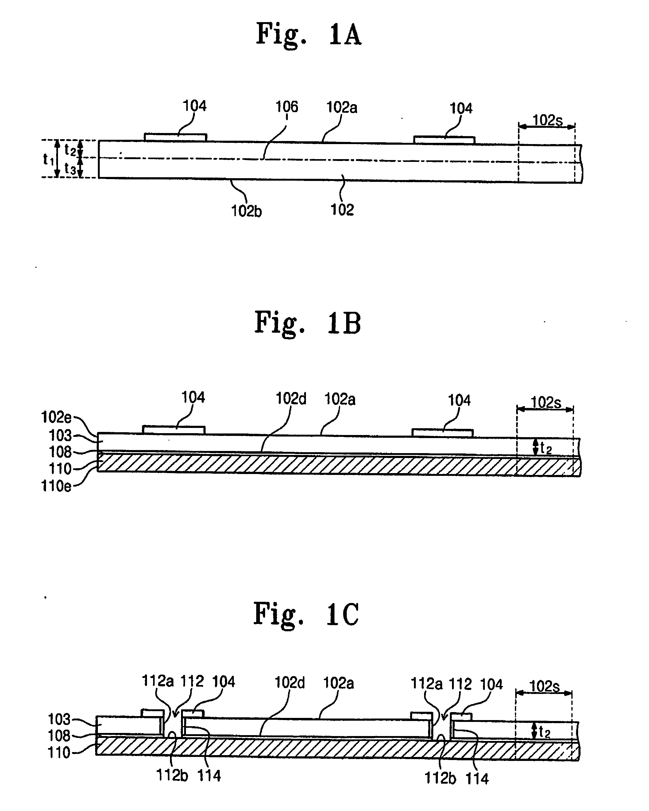
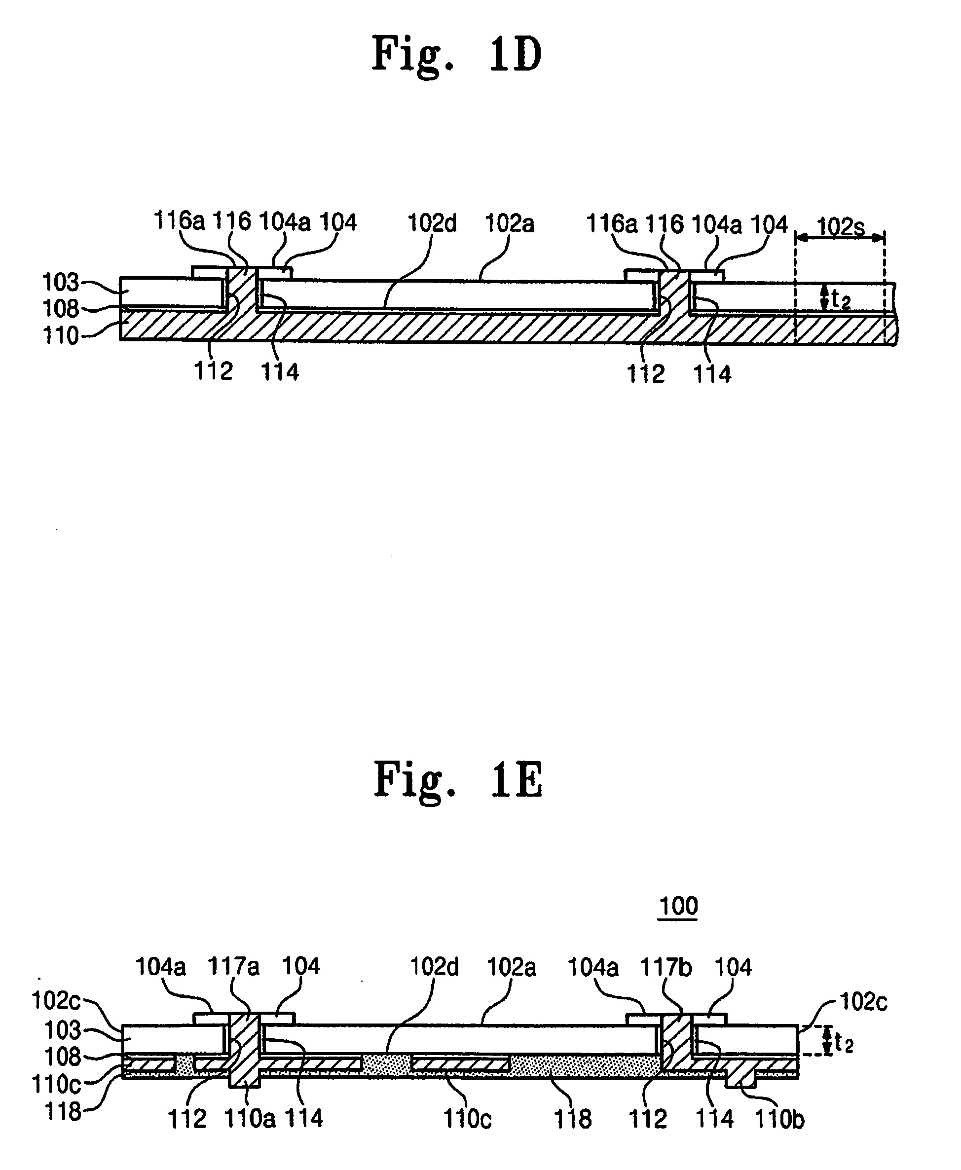
[0036]FIGS. 1A through 1E illustrate cross-sectional views of stages in a method of fabricating a chip package, e.g., a wafer level package, for a 3-D device package according to a Referring to FIG. 1A, a wafer 102 having a thickness ti may be prepared. The wafer 102 may include, e.g., conductive pads 104 for providing connections, e.g., signals, power, ground, etc., to devices formed on an active surface 102a of the wafer 102. The devices may include transistors, resistors, capacitors, etc. The wafer 102 may be, e.g., a semiconductor wafer, an opto-electronic wafer having optical and electronic devices thereon, etc. The wafer 102 may include a plurality of device patterns replicated thereon and corresponding to individual dies. The wafer 102 may be designed with scribe lanes 102s, i.e., dicing lanes, to facilitate separation of the wafer 102 into individual dies.

[0037]The wafer 102 may be processed to remove a predetermined portion of its thickness from a rear surface 102b thereof...

third embodiment

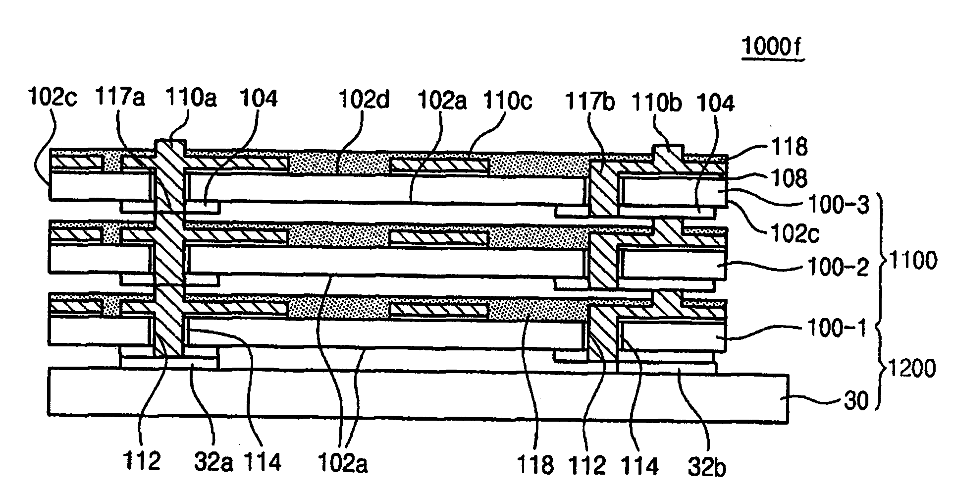
[0054]FIG. 3 illustrates a chip package 100a according to a Referring to FIG. 3, each of the connection pads 110a and 110b may extend laterally away from the respective through-hole electrodes 117a and 117b so as to redistribute the pad connections. Thus, a pitch of the connection pads 110a, 110b may be enlarged relative to the pitch of the corresponding connections to the thinned wafer 103. In an implementation, a heat sink 110c may also be formed in, e.g., a central region of the thinned wafer 103, by patterning the carrier 110.

fourth embodiment

[0055]FIG. 4 illustrates a chip package 100b according to a Referring to FIG. 4, each of the connection pads 110a and 110b may be arranged directly below the corresponding through-hole electrodes 117a and 117b. The connection pads 110a and 110b may be used to couple to corresponding pads on an adjacent chip package, as described below. In an implementation, one or more heat sinks 110c may also be formed, e.g., in central and peripheral regions of the thinned wafer 103, by patterning the carrier 110.


PUM

PropertyMeasurementUnit
aspect ratiosaaaaaaaaaa
electrically insulatingaaaaaaaaaa
semiconductoraaaaaaaaaa

Abstract

A method of fabricating a semiconductor device includes providing a semiconductor substrate having an active surface, thinning the substrate by removing material from a second surface of the substrate opposite the active surface, bonding a metal carrier to the second surface of the thinned substrate, forming a via opening in the thinned substrate, forming a conductive member in the via opening, and patterning the metal carrier bonded to the second surface of the thinned substrate to form a metal pattern.

Description

BACKGROUND OF THE INVENTION[0001]1. Field of the Invention[0002]Embodiments relate to a method of fabricating a three-dimensional (3-D) device and a device made thereby, e.g., a device in which one or more substrates are arranged in a stack.[0003]2. Description of the Related Art[0004]The development of next-generation electronic devices requires advances in packaging to enable the manufacture of reliable, compact, high performance devices. Further, cost-effective manufacturing of such devices depends on the ability to employ manufacturing processes that are robust and provide high yields. There are a wide variety of packages that have been developed. Existing packages, however, may not fulfill all of the above-described requirements for next-generation devices.SUMMARY OF THE INVENTION[0005]Embodiments are therefore directed to a method of fabricating a 3-D device and a device made thereby, which substantially overcome one or more of the problems due to the limitations and disadvant...

Claims


Application Information

Patent Timeline
Patent Type & Authority Applications(United States)
IPC IPC(8): H01L23/52H01L21/00H01L21/44
CPCH01L21/76898H01L23/525H01L25/0657H01L25/50H01L2225/06589H01L2225/06513H01L2225/06527H01L2225/06541H01L2224/16145H01L23/12
Inventor LEE, JONG HOLEE, DONG HOAHN, EUN CHULKWON, YONG CHAI
Owner SAMSUNG ELECTRONICS CO LTD
Why Eureka
Try Eureka