Display module and tiled display manufacturing method

a technology of display module and manufacturing method, which is applied in the manufacture of electric discharge tube/lamps, discharge tube luminescent screens, instruments, etc., can solve the problems of not being able to provide sufficient high resolution at the same time, unable to achieve large size of display, and unable to achieve high resolution

Inactive Publication Date: 2009-02-05
KIRYUSCHEV IRINA +1
View PDF15 Cites 22 Cited by
  • Summary
  • Abstract
  • Description
  • Claims
  • Application Information

AI Technical Summary

Benefits of technology

[0022]According to yet another aspect of the invention, there is provided a method for use in fabricating a display module for a multi-module flat panel display device in the form of a matrix of pixels formed by active media enclosed between two sets of conductors, the method comprising bending each of the conductors of at least one set of conductors in at least one end th

Problems solved by technology

However, a display having both large size and high resolution is difficult to obtain.
The known Liquid Crystal, Electroluminescent and Plasma Displays on solid or film substrates cannot practically be made very large and provide sufficiently high resolution at the same ti

Method used


Image

  • Display module and tiled display manufacturing method
  • Display module and tiled display manufacturing method
  • Display module and tiled display manufacturing method

Examples


Embodiment Construction

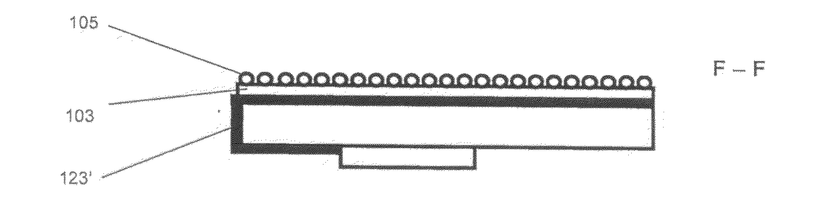
[0041]Reference is made to FIGS. 4A and 4B schematically illustrating a tiled display device 100 according to an example of the present invention. As shown in FIG. 4A, the display device is formed by multiple tiles (subdisplays)—four such subdisplays 101A-101D in the present example. Generally, the subdisplay of the present invention is configured as a passive matrix display including two sets of electrical conductors (termed X- and Y-sets) extending along two intersecting axes, respectively, and active media. The active media and the conductors are arranged to define together the subdisplay body. The X- and Y-sets of conductors define a two dimensional array of junctions. For example, such a subdisplay body may be carried on a substrate, solid or flexible.

[0042]In the present example, the device 100 includes a substrate 104 carrying conductors 105 from Y-set of conductors, conductors 102 from X-set of conductors, and electro-luminescent or electro-light-modulating media 103. Also, ...


PUM


Abstract

A flat panel display device is presented. The device includes at least one display module in the form of a matrix of pixels formed by active media enclosed between two sets of conductors. The display module has a front side by which it is to be exposed to viewers and an opposite back side where an electronic control circuit is located, and comprises two sets of electrical conductors extending along two intersecting axes respectively to define a two-dimensional array of junctions forming said pixels, each of the conductors of at least one set of conductors being bent to extend from the front side to the opposite back side of the display module.

Description

FIELD OF THE INVENTION[0001]The present invention is generally in the field of flat panel displays and relates to tiled flat displays of arbitrary size and high resolution.BACKGROUND OF THE INVENTION[0002]Existing flat displays are of different types including those utilizing the so-called “passive matrix” formed by an active medium (e.g. electro-light-modulating, such as liquid crystal, or electro-luminescent structure) enclosed between two sets of electrodes, and “active matrix” configuration formed by an active medium adjacent to electrodes and transistor-based arrangements. Known flat panel displays may be configured either with large size, or configured to provide high resolution of a displayed image. However, a display having both large size and high resolution is difficult to obtain.[0003]FIG. 1 graphically shows (in logarithmic coordinates) a relation between the resolution and display size for modern displays of different types, namely plasma display, LCD display, LCD TV di...

Claims


Application Information

Patent Timeline
IPC IPC(8): G02F1/1345H01J1/62H01J9/24H01L33/00
CPCG02F1/13336G06F3/1446H05B33/26G09G2380/02G06F3/147G02F1/1345H04N9/44
Inventor KIRYUSCHEV, IRINAKONSTEIN, SEMYON
Owner KIRYUSCHEV IRINA
Why Eureka
Try Eureka