Substrate and manufacturing method of the same, and semiconductor device and manufacturing method of the same

a manufacturing method and semiconductor technology, applied in the direction of solid-state devices, electrical apparatus construction details, basic electric elements, etc., can solve the problems of affecting the decrease of manufacturing cost, mold resin is less flexible the underfill, mold resin is harder than the solder resist,

Inactive Publication Date: 2009-02-05
SEIKO EPSON CORP
View PDF6 Cites 48 Cited by
  • Summary
  • Abstract
  • Description
  • Claims
  • Application Information

AI Technical Summary

Benefits of technology

[0036]In such structure, even in a case where the plurality of metal columns have the same shape, the same dimension, and the same color as each other, for example, a metal column to which the first conductive member that is wire-like is to be attached (that is, the second metal column) can be correctly recognized based on the recognition mark. Therefore, the first conductive member that is wire-like can be accurately attached to the second metal column.

Problems solved by technology

Especially, in terms of products in low-volume high-mix production, a lot of lead frames, substrates, or photo-masks are required for respective produce of the products, interfering the decrease of the manufacturing cost.
That is, the mold resin is less flexible than the solder resist and the underfill.
That is, the mold resin is harder than the solder resist and the underfill.

Method used


Image

  • Substrate and manufacturing method of the same, and semiconductor device and manufacturing method of the same
  • Substrate and manufacturing method of the same, and semiconductor device and manufacturing method of the same
  • Substrate and manufacturing method of the same, and semiconductor device and manufacturing method of the same

Examples


first embodiment

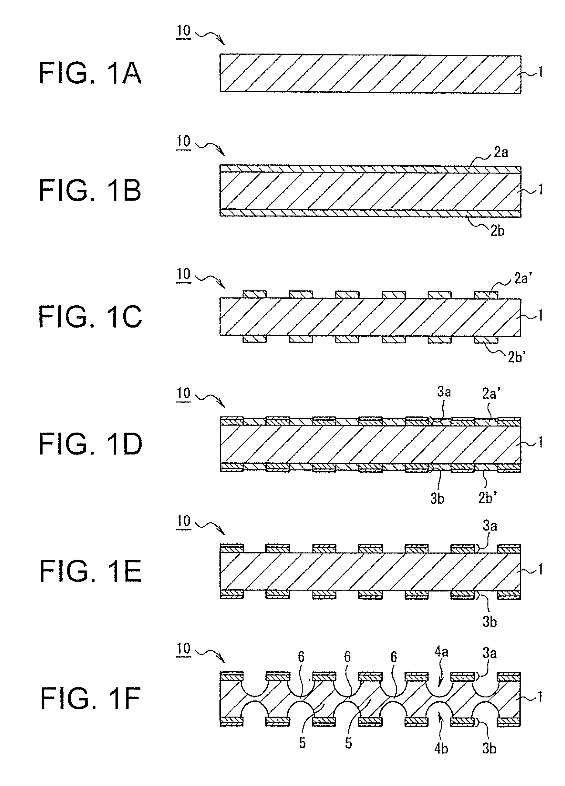
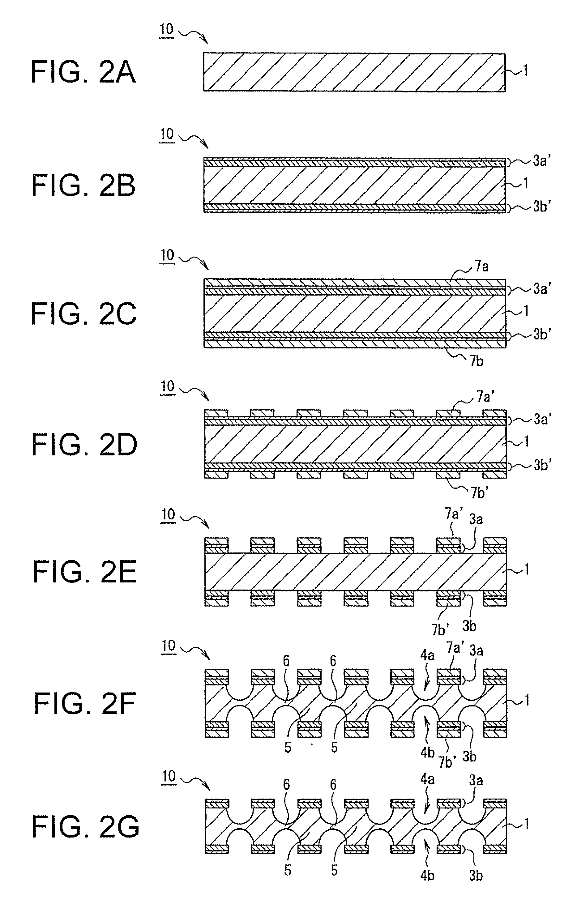
[0082]In a first embodiment, a method for manufacturing a substrate will be first described, and a method for manufacturing a semiconductor device by attaching an integrated circuit (IC) element to the substrate will be next described. The first embodiment will describe two types of manufacturing methods that are shown in FIGS. 1A through 1F and 2A through 2G as examples of a method for manufacturing a substrate. FIGS. 1A through 1F show a manufacturing method applying a semi-additive method, and FIGS. 2A through 2G show a manufacturing method applying a subtractive method. After these two types of manufacturing methods are described, processes of attaching an IC element and resin-sealing will be described with reference to FIGS. 3A through 3E, and a dicing process will be described with reference to FIGS. 4A and 4B.

[0083]FIGS. 1A through 1F are sectional views showing a method (a semi-additive method) for manufacturing a substrate 10 according to a first embodiment of the invention...

second embodiment

[0129]FIGS. 8A through 8C are sectional views showing a method for manufacturing a semiconductor device 110 according to a second embodiment of the invention. Such case will be described below that after the back surface penetration shown in FIG. 3E (that is, after the connecting part 6 is removed), the concave part 4b formed on the back surface side of the substrate 10 is filled with a resist, and Ni, Pd, and Au plating or Ni and Au plating is used as the plating layer 3b on the back surface, or a solder plating is additionally formed on the plating layer 3b. In FIGS. 8A through 8C, portions having the same structure as those described in the first embodiment have the same reference numerals, and detailed descriptions thereof will be omitted.

[0130]Referring to FIG. 8A, the process up to the back surface penetration step is same as that in the first embodiment. This second embodiment applies a solder resist 16 on the back surface side of the substrate 10 after the back surface penet...

third embodiment

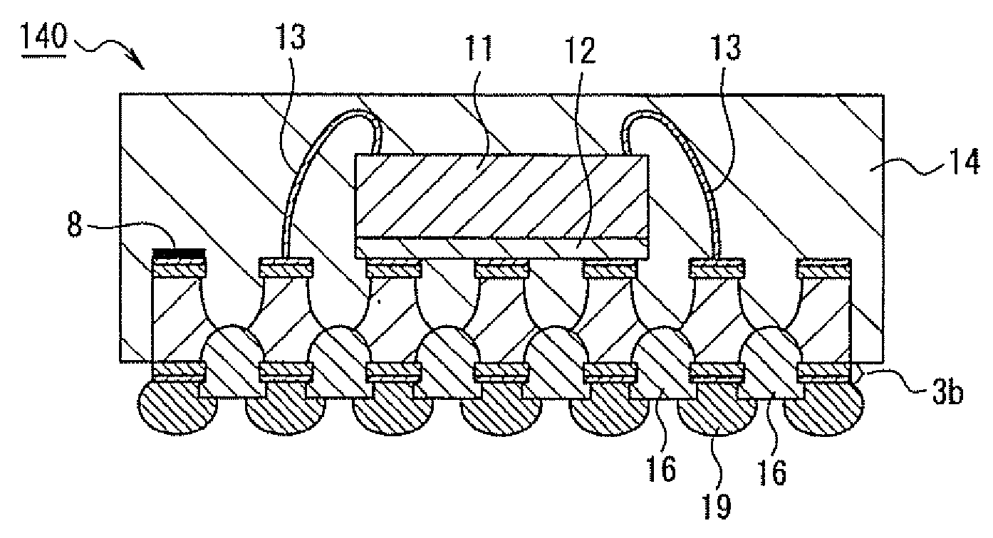
[0139]FIGS. 9A through 9C are sectional views showing a method for manufacturing a semiconductor device 120 according to a third embodiment of the invention. Such case will be described below that after the back surface penetration in FIG. 3E (that is, after the connecting part 6 is removed), the concave part 4b formed on the back surface side of the substrate 10 is filled with the solder resist 16 and a solder ball 19 is mounted on the plating layer 3b. In FIGS. 9A through 9C, portions having the same structure as those described in the first and second embodiments have the same reference numerals, and detailed descriptions thereof will be omitted.

[0140]Referring to FIG. 9A, the process up to the back surface penetration step is same as that in the first embodiment. This third embodiment applies the solder resist 16 on the back surface of the substrate 10 after the back surface penetration so as to fill the concave part 4b. In the third embodiment, the solder resist 16 is applied t...


PUM

PropertyMeasurementUnit
thicknessaaaaaaaaaa
depthaaaaaaaaaa
depthaaaaaaaaaa

Abstract

A substrate for fixing an integrated circuit element includes: a plurality of metal columns that are aligned in a longitudinal direction and a lateral direction in a planar view, each of the plurality of metal columns having a first face and a second face facing opposite direction to the first face; and a connecting part that connects the plurality of metal columns one another at a part of each of the plurality of metal columns between the first face and the second face. In the substrate, a recognition mark is formed on the first face of one of the plurality of metal columns.

Description

[0001]The entire disclosure of Japanese Patent Application No. 2007-199565, filed Jul. 31, 2007 is expressly incorporated by reference herein.BACKGROUND[0002]1. Technical Field[0003]The present invention relates to a substrate and a manufacturing method of the same, and a semiconductor device and a manufacturing method of the same.[0004]2. Related Art[0005]Semiconductor packages are classified broadly into a peripheral type package in which external terminals are arranged at the periphery of the package and an area type package in which external terminals are disposed at the under surface of the package. Packages typified by DIP (dual inline package), SOP (small outline package), and QFP (quad flat package) are the peripheral type package, as shown in FIGS. 40A through 40C. As shown in FIG. 40D, the peripheral type package is manufactured such that an integrated circuit (IC) element 210 is mounted on a die pad 201 that is a chip mounting part, an electrode provided on the IC element...

Claims


Application Information

Patent Timeline
Patent Type & Authority Applications(United States)
IPC IPC(8): H01L21/50H05K7/02
CPCH01L21/4832H01L21/563H01L21/568H01L21/6835H01L23/3107H01L23/544H01L24/32H01L24/45H01L24/48H01L24/81H01L24/83H01L24/90H01L24/97H01L25/16H01L2221/68345H01L2221/68377H01L2223/54426H01L2223/54473H01L2224/16245H01L2224/32245H01L2224/45144H01L2224/48091H01L2224/48095H01L2224/48227H01L2224/48247H01L2224/484H01L2224/48599H01L2224/49171H01L2224/73203H01L2224/73265H01L2224/81121H01L2224/81801H01L2224/83191H01L2224/83855H01L2224/85001H01L2224/92247H01L2224/97H01L2924/01004H01L2924/01005H01L2924/01028H01L2924/01029H01L2924/01033H01L2924/01046H01L2924/01047H01L2924/0105H01L2924/01078H01L2924/01079H01L2924/01082H01L2924/014H01L2924/07802H01L2924/14H01L2924/15311H01L2924/18301H01L2924/19043H01L2924/19105H01L2924/3025H01L24/49H01L2224/2919H01L2924/01006H01L2924/01075H01L2924/0665H01L2224/16225Y10T29/4921H01L2924/00014H01L2224/85H01L2224/83H01L2224/81H01L2924/00012H01L2924/00H01L2924/15788H01L2924/181H01L24/73H01L2224/85399H01L2224/05599H01L23/48
Inventor SHOJI, MASANOBUFUJITA, TORU
Owner SEIKO EPSON CORP
Why Eureka
Try Eureka