Pattern measurement apparatus

a technology of pattern measurement and measurement apparatus, which is applied in the field of pattern measurement apparatus, can solve the problems of increasing difficulty in involving, within the field of view, the entire pattern, or a range, and difficulty in establishing mutual compatibility between high-magnification observation for high-resolution implementation and observation in a wide region, and the technology is unsuitable for accomplishmen

Active Publication Date: 2009-02-12
HITACHI HIGH-TECH CORP
View PDF8 Cites 48 Cited by
  • Summary
  • Abstract
  • Description
  • Claims
  • Application Information

AI Technical Summary

Benefits of technology

[0010]According to the above-described configuration, it turns out that the identification information is added to each fragment on the SEM image which has possessed no specific identification information originally. As a consequence, it becomes possible to implement the management of the SEM image based on the identification information. Giving an example, a case is considered where a superimposed image is formed by mutually connecting images of a plurality of field-of-views to each other. In this case, at the time of the formation, the mutual

Problems solved by technology

If, however, the measurement is made using the high magnification needed for evaluating a location like this, there occurs the following problem: Namely, it becomes increasingly difficult to involve, within the field-of-view, the entire pattern, or a range of the pattern needed at least for identifying configuration of the pattern.
As a c

Method used


Image

  • Pattern measurement apparatus
  • Pattern measurement apparatus
  • Pattern measurement apparatus

Examples


Embodiment Construction

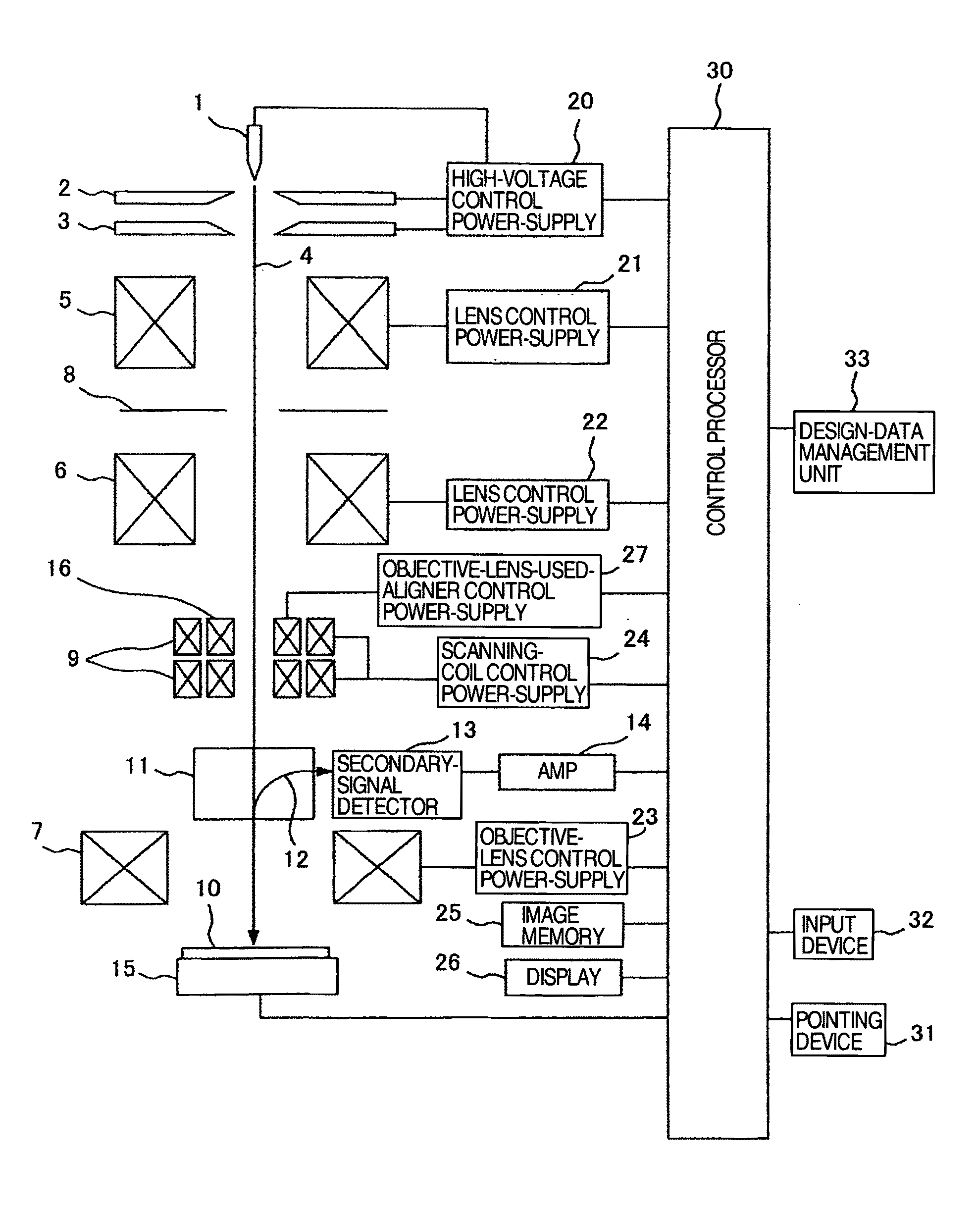
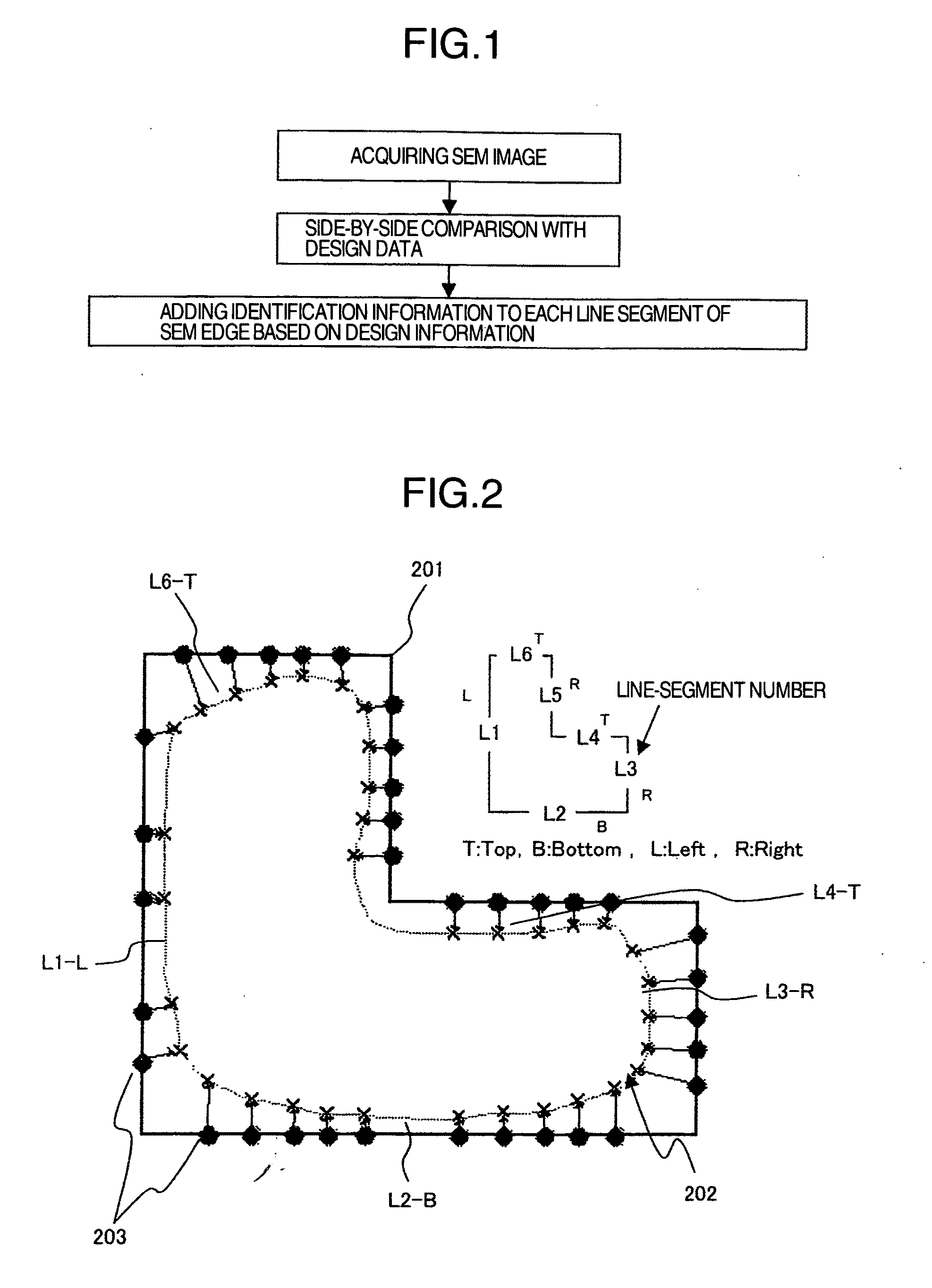
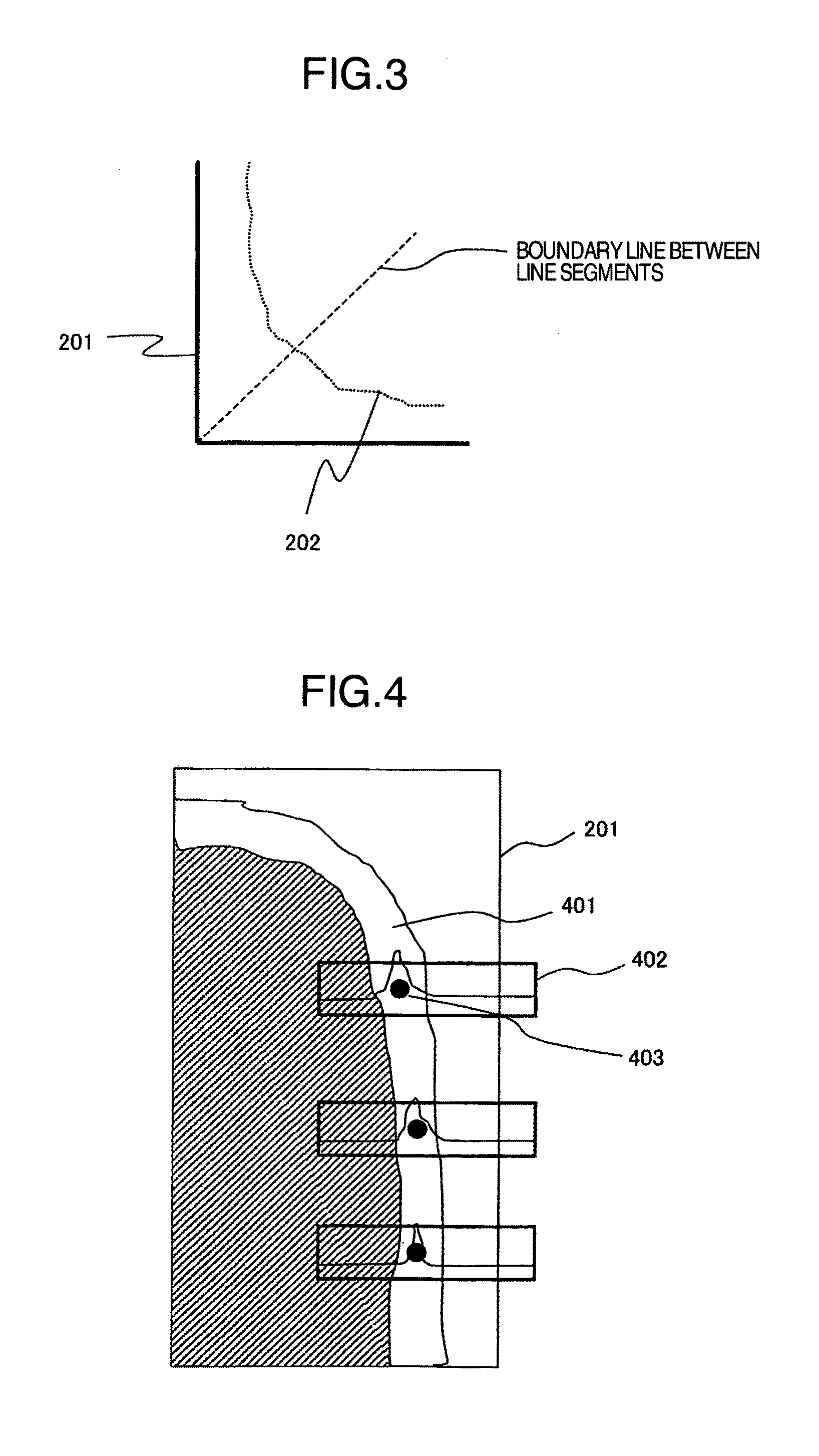
[0033]Hereinafter, the explanation will be given below concerning the following embodiment: A side-by-side checking (i.e., comparison) is made between the edge portion of a SEM (: Scanning Electron Microscope) image formed by an electron microscope and the design data, thereby adding identification information to the SEM edge which constitute each fragment of the pattern. In FIG. 1, the SEM edge is extracted from a SEM image formed by an electron microscope, then making a side-by-side checking between each line segment of the SEM edge and the design data. The design data includes a variety of information about the pattern. In the present embodiment, however, information specific to each line segment constituting the pattern is extracted in particular out of this variety of information. Then, the information extracted is applied as the identification information for each fragment. FIG. 2 is a diagram for explaining an embodiment where the identification information is added to the SE...


PUM


Abstract

Mutual compatibility is established between the measurement with a high magnification and the measurement in a wide region. A pattern measurement apparatus is proposed which adds identification information to each of fragments that constitute a pattern within an image obtained by the SEM, and which stores the identification information in a predetermined storage format. Here, the identification information is added to each fragment for distinguishing between one fragment and another fragment. According to the above-described configuration, it turns out that the identification information is added to each fragment on the SEM image which has possessed no specific identification information originally. As a result, it becomes possible to implement the SEM-image management based on the identification information.

Description

BACKGROUND OF THE INVENTION[0001]The present invention relates to an apparatus for making measurement and inspection of a pattern based on design data on a semiconductor device or the like and the image obtained by a scanning electron microscope. More particularly, it relates to a pattern measurement apparatus for adding identification information to line segments within the electron-microscope image, and managing the pattern-forming line segments based on the identification information.[0002]In recent years, the design data on a semiconductor device has increasingly come into use for the measurement on the semiconductor device by the scanning electron microscope (: SEM). In JP-A-2006-66478 (corresponding to US 2006 / 0045326), the following embodiment is explained: A pattern matching is performed between line segments based on the design data and contour lines of patterns obtained by the scanning electron microscope. Then, a pattern is measured which is identified by this pattern mat...

Claims


Application Information

Patent Timeline
IPC IPC(8): G01N23/00
CPCG03F7/70616G06T7/0006G06T2207/10061G06T2207/30148H01J2237/2817H01J37/28H01J2237/221H01J2237/24592H01J37/222
Inventor MATSUOKA, RYOICHIONIZAWA, AKIHIROSUGIYAMA, AKIYUKIMOROKUMA, HIDETOSHITOYODA, YASUTAKA
Owner HITACHI HIGH-TECH CORP
Why Eureka
Try Eureka