Mounting assembly of semiconductor packages prevent soldering defects caused by substrate warpage

a technology of mounting assembly and semiconductor packages, which is applied in the direction of printed circuit aspects, sustainable manufacturing/processing, final product manufacturing, etc., can solve the problems of warpage of semiconductor package substrates, soldering defects, cold soldering, etc., and achieve the effect of reducing stacking standoffs

Inactive Publication Date: 2009-02-12
POWERTECH TECHNOLOGY
View PDF8 Cites 19 Cited by
  • Summary
  • Abstract
  • Description
  • Claims
  • Application Information

AI Technical Summary

Benefits of technology

[0033]The compensating bumps 440 are selectively disposed either on the first connecting pads 423 or on the second connecting pads 424 to compensate the stacking standoff differences between the second external terminals 414 and the first external terminals 413 when the first semiconductor package 410 is mounted on the package carrier 420. It is to reduce the stacking standoffs between the first external terminals 413 and the first connecting pads 423 and between the second external terminals 414 and the se...

Problems solved by technology

As the thickness requirements of POP semiconductor packages become thinner and thinner, the warpage of the substrates of semiconductor packages become worse and worse leading to soldering defects such as cold soldering, empty soldering, and fault soldering.
Soldering defects beco...

Method used


Image

  • Mounting assembly of semiconductor packages prevent soldering defects caused by substrate warpage
  • Mounting assembly of semiconductor packages prevent soldering defects caused by substrate warpage
  • Mounting assembly of semiconductor packages prevent soldering defects caused by substrate warpage

Examples


first embodiment

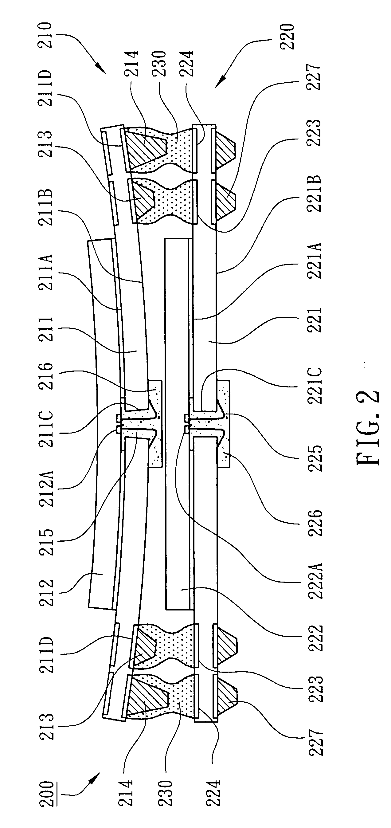
[0016]According to the present invention, as shown in FIG. 2, a mounting assembly 200 of semiconductor packages primarily comprises at least a first semiconductor package 210, a package carrier 220, and solder paste 230 where the first semiconductor package 210 is mounted on top of the package carrier 220 and is electrically connected to the package carrier 220 by solder paste 230.

[0017]The first semiconductor package 210 includes a first substrate 211, a first chip 212, a plurality of first external terminals 213, and a plurality of second external terminals 214. The first substrate 211, such as printed circuit boards, acts as an electrically connecting medium of the first chip 212 to the package carrier 220. The first substrate 211 has a top surface 211 A and a bottom surface 211B. The first chip 212 is an IC fabricated on a Si wafer and may be a processor, a memory, a logic, an ASIC, or a multi-functional IC. The first external terminals 213 and the second external terminals 214 ...

fourth embodiment

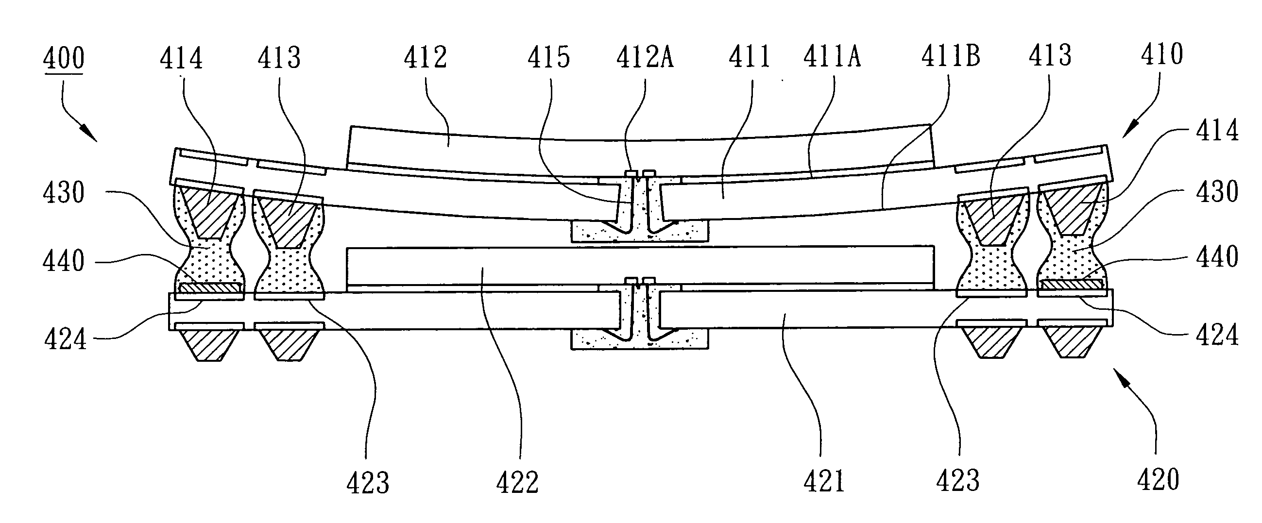
[0030]As shown in FIG. 6, another mounting assembly 400 of semiconductor packages is revealed according to the present invention, primarily comprising at least a semiconductor package 410, a package carrier 420, and solder paste 430, and further comprising a plurality of compensating bumps 440 on the package carrier 420.

[0031]The first semiconductor package 410 includes a first substrate 411, a first chip 412, a plurality of first external terminals 413, and a plurality of second external terminals 414 where the first external terminals 413 and the second external terminals 414 are disposed on a bottom surface 411B of the first substrate 411. The first chip 412 is disposed on a top surface 411A, but not limited, the first chip 412 may be disposed on the bottom surface 411B of the first substrate 411 or in a die cavity of the first substrate 411 (not shown in figures). The bonding pads 412A of the first chip 412 are electrically connected to the first substrate 411 by a plurality of ...


PUM


Abstract

A mounting assembly of semiconductor packages is revealed, primarily comprising at least a semiconductor package having a plurality of external terminals, a package carrier, and solder paste. The solder paste joints the external terminals to the package carrier. According to the distance to a central line on a substrate of the semiconductor package, the external terminals are divided into at least two different groups. In one of the embodiment, different groups of the external terminals are bumps with non-equal heights to achieve a uniform standoff plane to compensate the warpage of the substrate. The predicted substrate warpage can be compensated without causing any soldering defects. In another embodiment, a plurality of compensating bumps are selectively disposed on one group of the external terminals with larger stacking gaps.

Description

FIELD OF THE INVENTION[0001]The present invention relates to the assembling technologies of semiconductor packages, especially to a mounting assembly of semiconductor packages to prevent soldering defects caused by substrate warpage which can be implemented in 3D packaging of Package-On-Package device (POP).BACKGROUND OF THE INVENTION[0002]As the thickness requirements of POP semiconductor packages become thinner and thinner, the warpage of the substrates of semiconductor packages become worse and worse leading to soldering defects such as cold soldering, empty soldering, and fault soldering. Soldering defects become a serious issue, especially in 3D stacking of semiconductor packages (or called POP device). In the miniature development of electronic products, a plurality of semiconductor packages can be vertically stacked to meet the requirements of higher density devices with smaller footprints. However, electrical connections between two electrical terminals of POP stacking will ...

Claims


Application Information

Patent Timeline
IPC IPC(8): H01L23/12
CPCH01L23/13H01L23/49816H01L2924/10253H01L2224/73215H01L24/48H01L2225/1058H01L2225/1023H01L2924/15311H01L2224/32225H05K2201/09736H05K2201/094H05K2201/09136H01L23/49838H01L25/105H01L2224/4824H01L2924/01079H01L2924/1433H01L2924/15331H01L2924/3511H05K3/3436H05K2201/0367H01L2924/00012H01L2924/00H01L2924/00014Y02P70/50H01L2224/45099H01L2224/45015H01L2924/207
Inventor FAN, WEN-JENG
Owner POWERTECH TECHNOLOGY
Why Eureka
Try Eureka