Method for manufacturing vertical mos transistor

Inactive Publication Date: 2009-02-12
LONGITUDE SEMICON S A R L
View PDF6 Cites 45 Cited by
  • Summary
  • Abstract
  • Description
  • Claims
  • Application Information

AI Technical Summary

Benefits of technology

[0040]forming a third insulating film having a thicker film thickness than a film thickness of the second insulating film or an insulating region having a thicker effective film thickness than a film thicknes

Problems solved by technology

With the miniaturization of semiconductor devices in recent years, the current driving ability of a MOS transistor making up a semiconductor device tends to decrease.
Also, a DRAM cell transistor i

Method used


Image

  • Method for manufacturing vertical mos transistor
  • Method for manufacturing vertical mos transistor
  • Method for manufacturing vertical mos transistor

Examples


first embodiment

A First Embodiment

[0068]A vertical MOS transistor of the first embodiment comprising:

[0069]a first insulating film between a lower impurity diffusion region in semiconductor substrate and a gate electrode; and

[0070]a gate insulating film between a protrusion-like region and a gate electrode,

[0071]wherein the film thickness of the first insulating film is thicker than the film thickness of a gate insulating film.

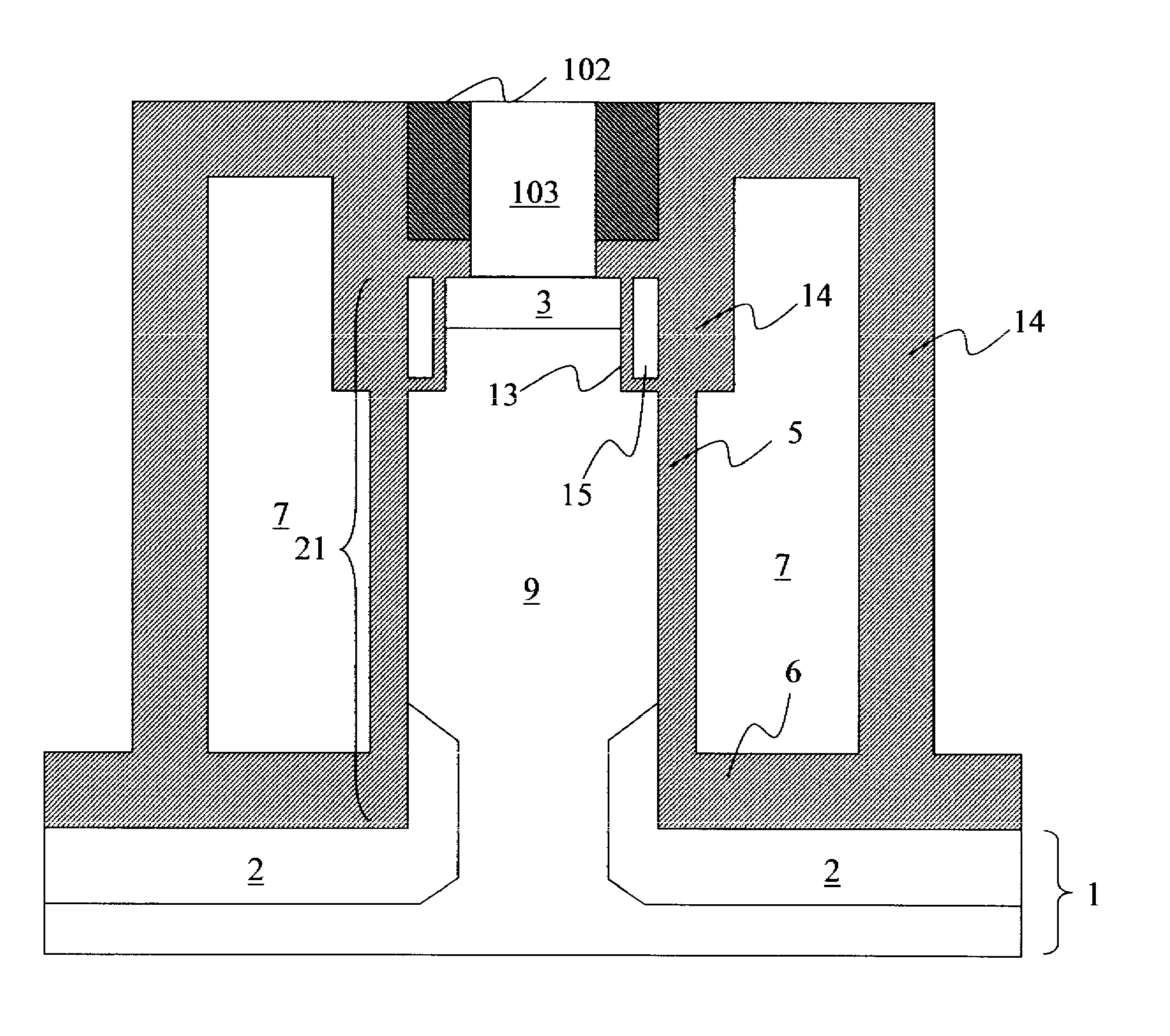
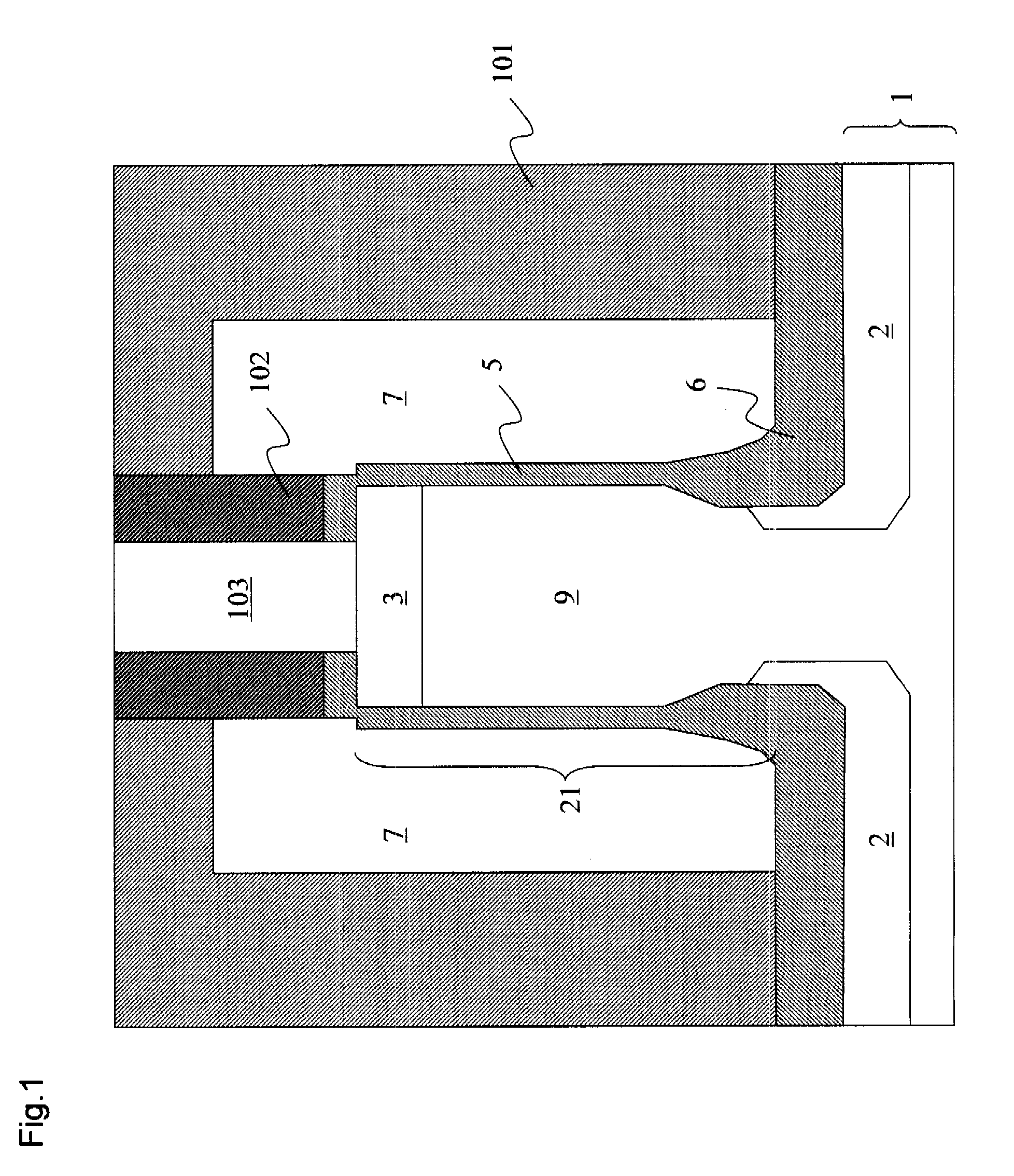
[0072]One example of this vertical MOS transistor is shown in FIG. 1. As shown in FIG. 1, protrusion-like region 21 is provided on P-type Si semiconductor substrate 1. Lower impurity diffusion region 2 is provided in a region from a lower portion in this protrusion-like region 21 into semiconductor substrate 1, and upper impurity diffusion region 3 is provided in an upper portion in protrusion-like region 21. Also, a channel region is formed between upper impurity diffusion region 3 and lower impurity diffusion region 2 in the protrusion-like region.

[0073]This lower impurity ...

second embodiment

A Second Embodiment

[0091]A vertical MOS transistor of the second embodiment comprising:

[0092]a first insulating film between a lower impurity diffusion region in semiconductor substrate and a gate electrode;

[0093]a gate insulating film constituted by a second insulating film between a channel region and a gate electrode; and

[0094]a third insulating film between an upper impurity diffusion region and a gate electrode,

[0095]wherein the film thickness of the first and the third insulating films is thicker than the film thickness of a gate insulating film.

[0096]One example of this vertical MOS transistor is shown in FIG. 8. As shown in FIG. 8, protrusion-like region 21 is provided on P-type Si semiconductor substrate 1. Lower impurity diffusion region 2 is provided in a region from a lower portion in this protrusion-like region 21 into semiconductor substrate 1, and upper impurity diffusion region 3 is provided in an upper portion in protrusion-like region 21. Also, a channel region is ...

third embodiment

A Third Embodiment

[0109]A vertical MOS transistor of the third embodiment comprising:

[0110]a first insulating film between a lower impurity diffusion region in semiconductor substrate and a gate electrode;

[0111]a gate insulating film constituted by a second insulating film between a channel region and a gate electrode; and

[0112]an insulating region constituted by a forth insulating film, a fifth insulating film and air gap region between an upper impurity diffusion region and a gate electrode,

[0113]wherein the film thickness of the first insulating film and the effective film thickness of the insulating region are thicker than the film thickness of a gate insulating film.

[0114]One example of vertical MOS transistor of this embodiment is shown in FIG. 16. As shown in FIG. 16, protrusion-like region 21 is provided on P-type Si semiconductor substrate (silicon semiconductor substrate) 1. Lower impurity diffusion region 2 is provided in a region from a lower portion in this protrusion-l...


PUM


Abstract

A method for manufacturing a vertical MOS transistor comprising forming a protrusion-like region, forming a silicon oxide film on an exposed surface of the protrusion-like region and a surface of the silicon semiconductor substrate, increasing a film thickness of at least the silicon oxide film on the silicon semiconductor substrate by thermal oxidation to form a first insulating film, forming a lower impurity diffusion region, removing the silicon oxide film to expose a silicon side of the protrusion-like region, thermally oxidizing the silicon side to form a second insulating film having a thinner film thickness than a film thickness of the first insulating film, forming a gate electrode over a side of the protrusion-like region, and forming an upper impurity diffusion region.

Description

[0001]This application is based upon and claims the benefit of priority from Japanese Patent Application No. 2007-208194, filed on Aug. 9, 2007, the disclosure of which is incorporated herein in its entirety by reference.BACKGROUND OF THE INVENTION[0002]1. Field of the Invention[0003]The present invention relates to a method for manufacturing a vertical MOS transistor.[0004]2. Description of the Related Art[0005]With the miniaturization of semiconductor devices in recent years, the current driving ability of a MOS transistor making up a semiconductor device tends to decrease. In order to improve this current driving ability, a vertical MOS transistor of a three-dimensional structure in which the source region, the channel region, and the drain region are vertically located is proposed. This vertical MOS transistor has the advantage that a significant improvement in current driving ability can be achieved by completely depleting the channel region.[0006]A related vertical MOS transis...

Claims


Application Information

Patent Timeline
IPC IPC(8): H01L29/78
CPCH01L29/0653H01L29/7827H01L29/66666H01L29/42368
Inventor OYU, KIYONORI
Owner LONGITUDE SEMICON S A R L
Why Eureka
Try Eureka