Display device and electronic equipment

a display device and electronic equipment technology, applied in semiconductor devices, instruments, electrical equipment, etc., can solve the problems of low power consumption, large high-definition display devices, and simple matrix display devices with some problems although simple, so as to prevent parasitic capacitance and minimize parasitic capacitance

Active Publication Date: 2009-02-19
SONY CORP
View PDF6 Cites 41 Cited by
  • Summary
  • Abstract
  • Description
  • Claims
  • Application Information

AI Technical Summary

Benefits of technology

[0022]In the display device configured as described above and electronic equipment having the same, the write scan line and, preferably, both the write scan line and the light emission control scan line do not intersect with the wiring pattern connected to the gate electrode of the drive transistor. This prevents parasitic capacitance from being coupled to the gate electrode of the drive t

Problems solved by technology

That is, it is low in power consumption because organic EL elements can be driven by a voltage of 10V or less.
It should be noted, however, that a simple matrix display device has some problems although simple in construction.
Such problems, include a difficulty in implementing a large high-definition display device becaus

Method used


Image

  • Display device and electronic equipment
  • Display device and electronic equipment
  • Display device and electronic equipment

Examples


modification example

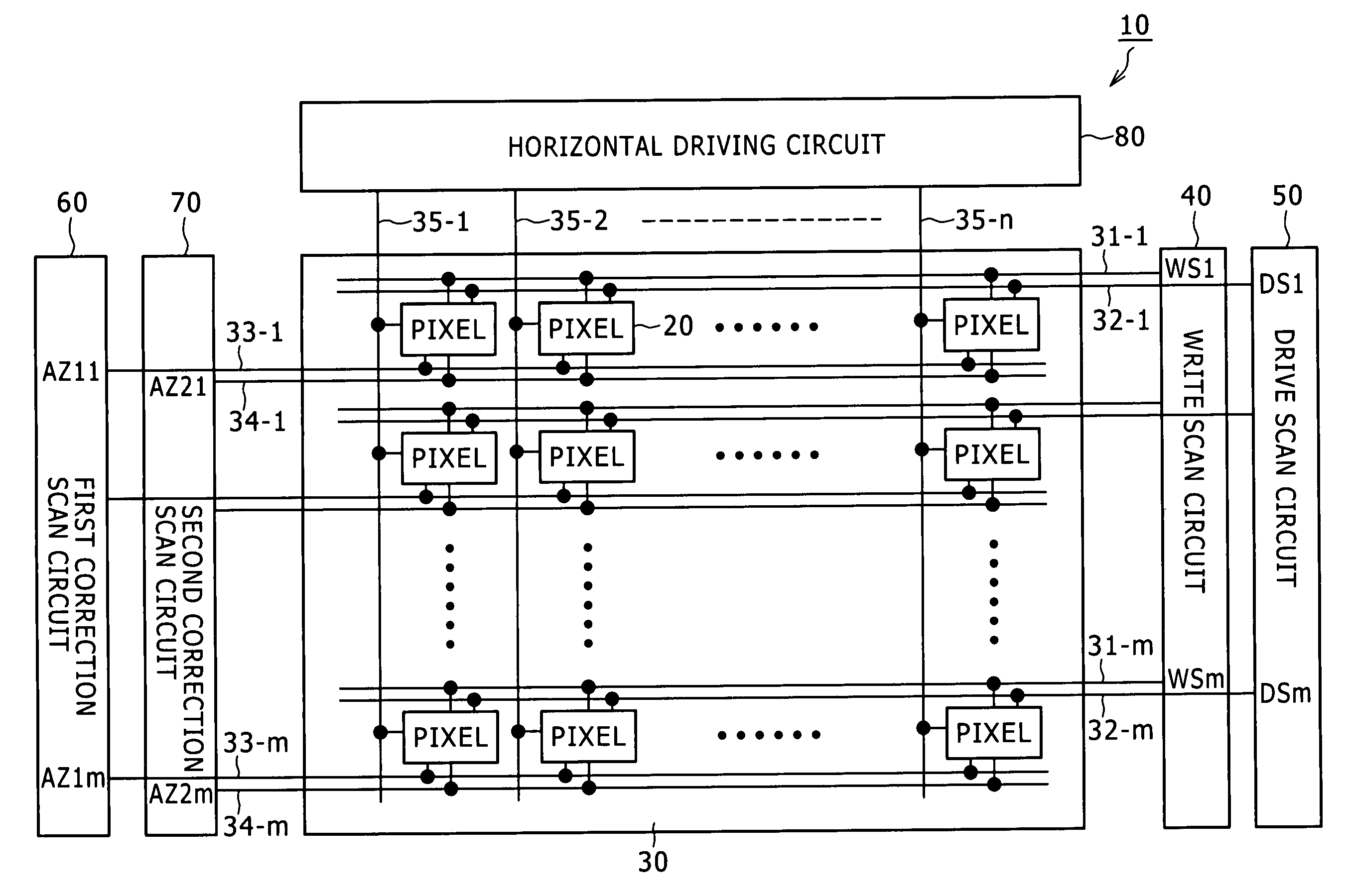
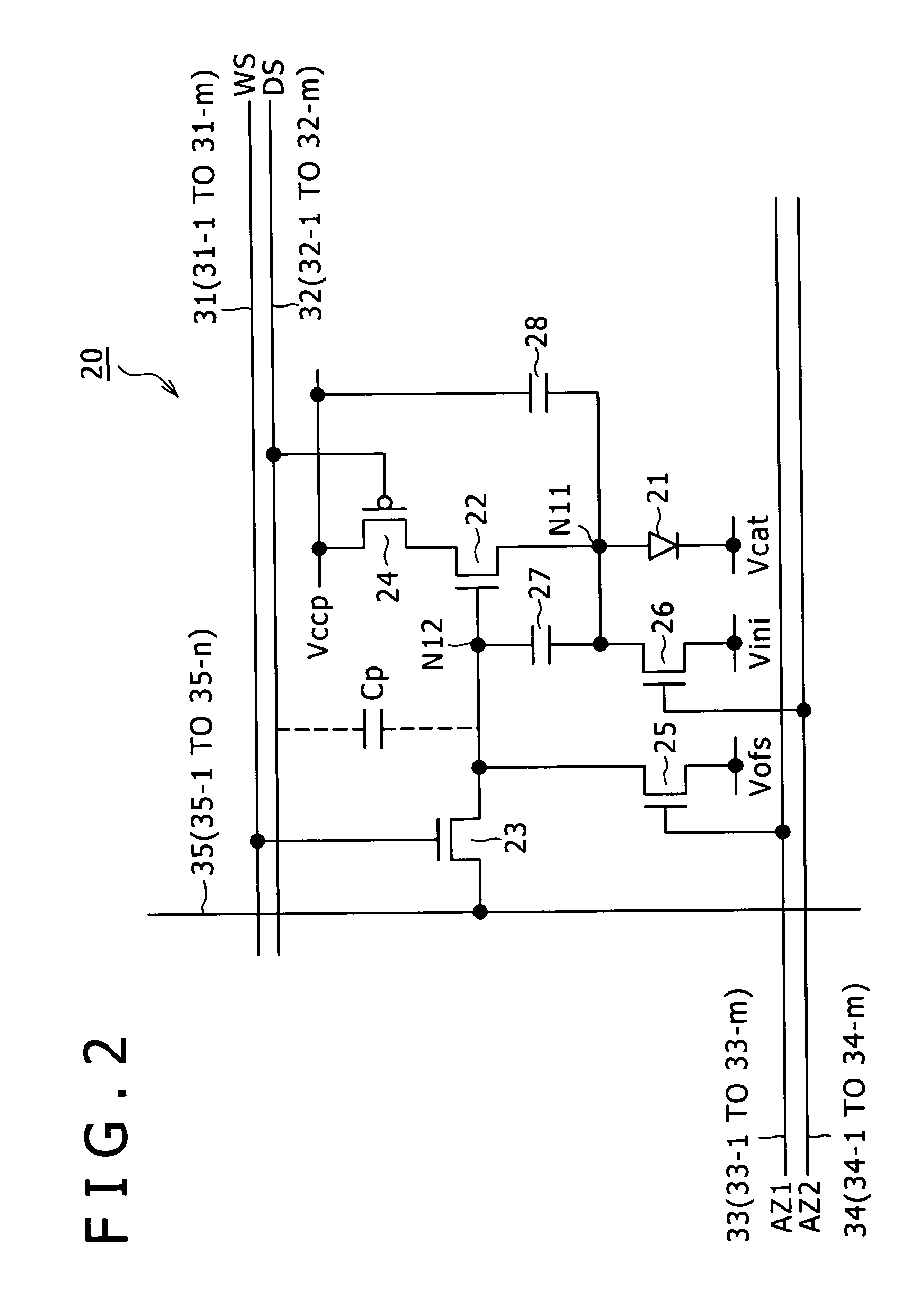
[0139]In the above embodiment, a description was given taking, as an example, the organic EL display device each of whose pixels contains five transistors, i.e., the drive transistor 22, the write transistor 23 and the switching transistors 24 to 26. However, the present invention is not limited to this application example, but in general is applicable to organic EL display devices having at least the drive transistor 22, the write transistor 23 connected to the gate electrode of the drive transistor 22 and the switching transistor 25.

[0140]Further, in the above embodiment, a description was given taking, as an example, the case in which the present invention was applied to an organic EL display device using organic EL elements. However, the present invention is not limited to this application example, but in general is applicable to flat panel display devices having pixels, each containing an electro-optical element, arranged in a matrix form.

application examples

[0141]The display device according to the present invention described above is applicable as a display device of electronic equipment across all fields, including those shown in FIGS. 9 to 13, namely, a digital camera, a laptop personal computer, a mobile terminal device such as mobile phone and a video camcorder. These pieces of equipment are designed to display an image or video of a video signal fed to or generated inside the electronic equipment.

[0142]As described above, if used as a display device of electronic equipment across all fields, the display device according to the present invention minimizes parasitic capacitance, a contributor to inhibiting the normal bootstrapping action, thus suppressing the reduction of light emission brightness caused by parasitic capacitance. This provides an improved image quality on the display screen in any type of electronic equipment.

[0143]It should be noted that the display device according to the present invention includes a modular form...


PUM


Abstract

The present invention provides a display device including a pixel array section, the pixel array section having pixels arranged in a matrix form, each of the pixels including: an electro-optical element; a write transistor; a holding capacitance; a drive transistor; and a switching transistor; a write scan line disposed for each of pixel rows of the pixel array section and adapted to convey a write signal to be applied to the gate electrode of the write transistor; and a correction scan line, wherein the wiring structure of the write scan line does not intersect with the wiring pattern connected to the gate electrode of the drive transistor.

Description

CROSS REFERENCES TO RELATED APPLICATIONS[0001]The present invention contains subject matter related to Japanese Patent Application JP 2007-211624, filed in the Japan Patent Office on Aug. 15, 2007, the entire contents of which are incorporated herein by reference.BACKGROUND OF THE INVENTION[0002]1. Field of the Invention[0003]The present invention relates to a display device and electronic equipment and, more particularly, to a flat panel display device and electronic equipment having the same in which pixels, each incorporating an electro-optical element, are disposed in a matrix form.[0004]2. Description of Related Art[0005]In the field of image display devices, flat panel display devices having pixels (pixel circuits), each incorporating an electro-optical element, disposed in a matrix form, are rapidly becoming widespread. Among flat panel display devices, the development and commercialization of organic EL display devices using organic EL (Electro Luminescence) elements have be...

Claims


Application Information

Patent Timeline
IPC IPC(8): G09G3/30
CPCG09G3/3233G09G3/3291G09G2300/0426G09G2300/0439G09G2300/0819G09G2300/0852H01L27/1255G09G2320/043G09G3/3225G09G2300/08G09G2320/045H01L27/124G09G2300/0861H10K59/123H10K59/122H10K59/1213H10K59/131H10K59/1216G09G2300/0833G09G2310/0286G09G2320/0233H01L27/1222
Inventor TANIKAME, TAKAO
Owner SONY CORP
Why Eureka
Try Eureka