Vertical memory device and method of manufacturing the same

a technology of vertical memory and flash memory, which is applied in the direction of semiconductor devices, basic electric elements, electrical equipment, etc., can solve the problems of unstable response and variable memory window size of the flash memory device, and achieve the effect of increasing the density of the charge trap pattern and reducing cross talk

Active Publication Date: 2018-02-01
SAMSUNG ELECTRONICS CO LTD
View PDF2 Cites 46 Cited by
  • Summary
  • Abstract
  • Description
  • Claims
  • Application Information

AI Technical Summary

Benefits of technology

[0008]Some example embodiments of inventive concepts provide a vertical memory device in which the charge trap pattern in a cell region and the dielectric inter-cell pattern in an inter-cell region are increased to thereby increase the trap density of the charge trap pattern and decrease the cross talk between the neighboring stack cells.

Problems solved by technology

Accordingly, the trap density in the charge trap pattern is not sufficient each cell of the vertical NAND flash memory device, which makes the memory window size of the flash memory device very variable and unstable in response to the size of the flash memory device.

Method used


Image

  • Vertical memory device and method of manufacturing the same
  • Vertical memory device and method of manufacturing the same
  • Vertical memory device and method of manufacturing the same

Examples


Embodiment Construction

[0029]Reference will now be made to some example embodiments, which are illustrated in the accompanying drawings, wherein like reference numerals may refer to like components throughout.

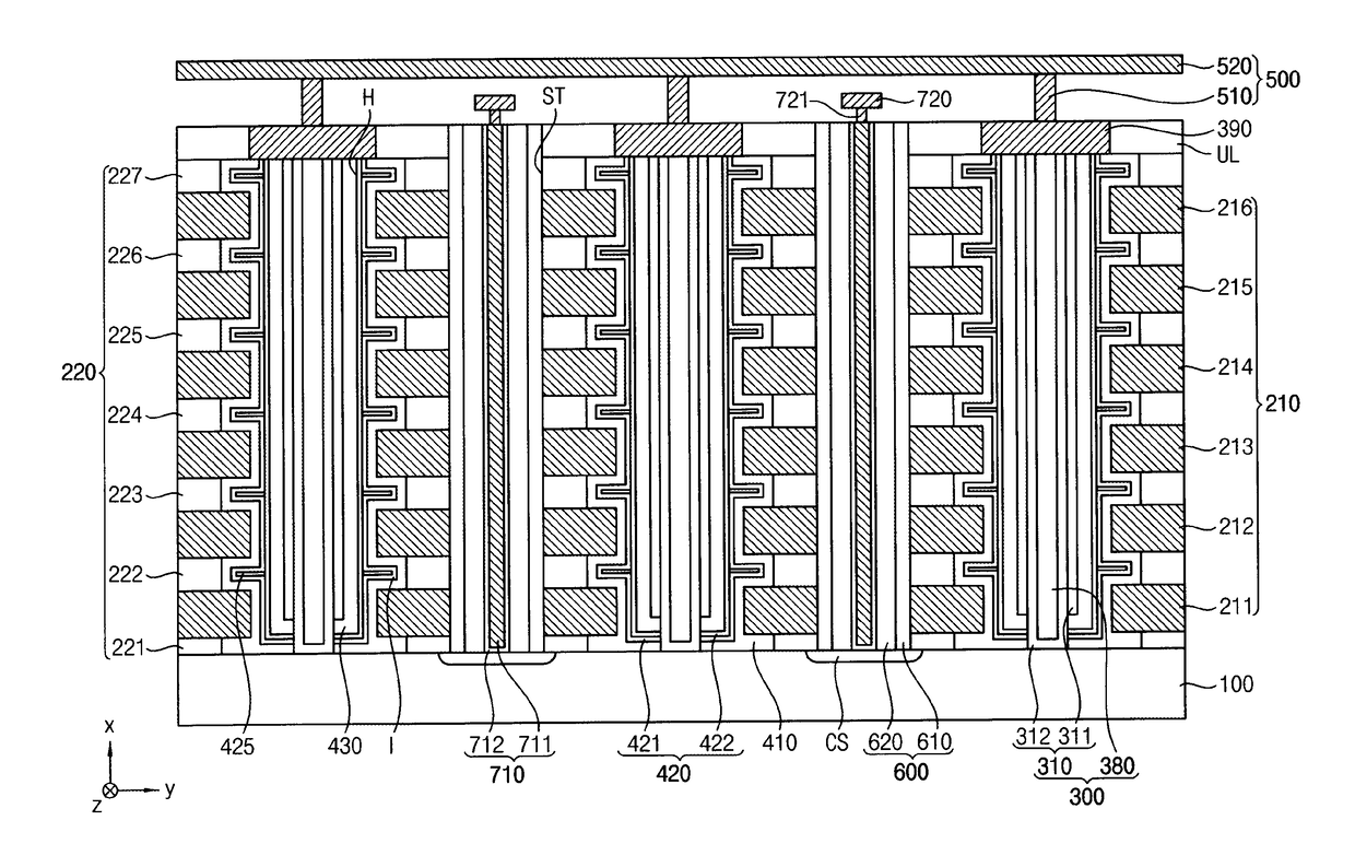
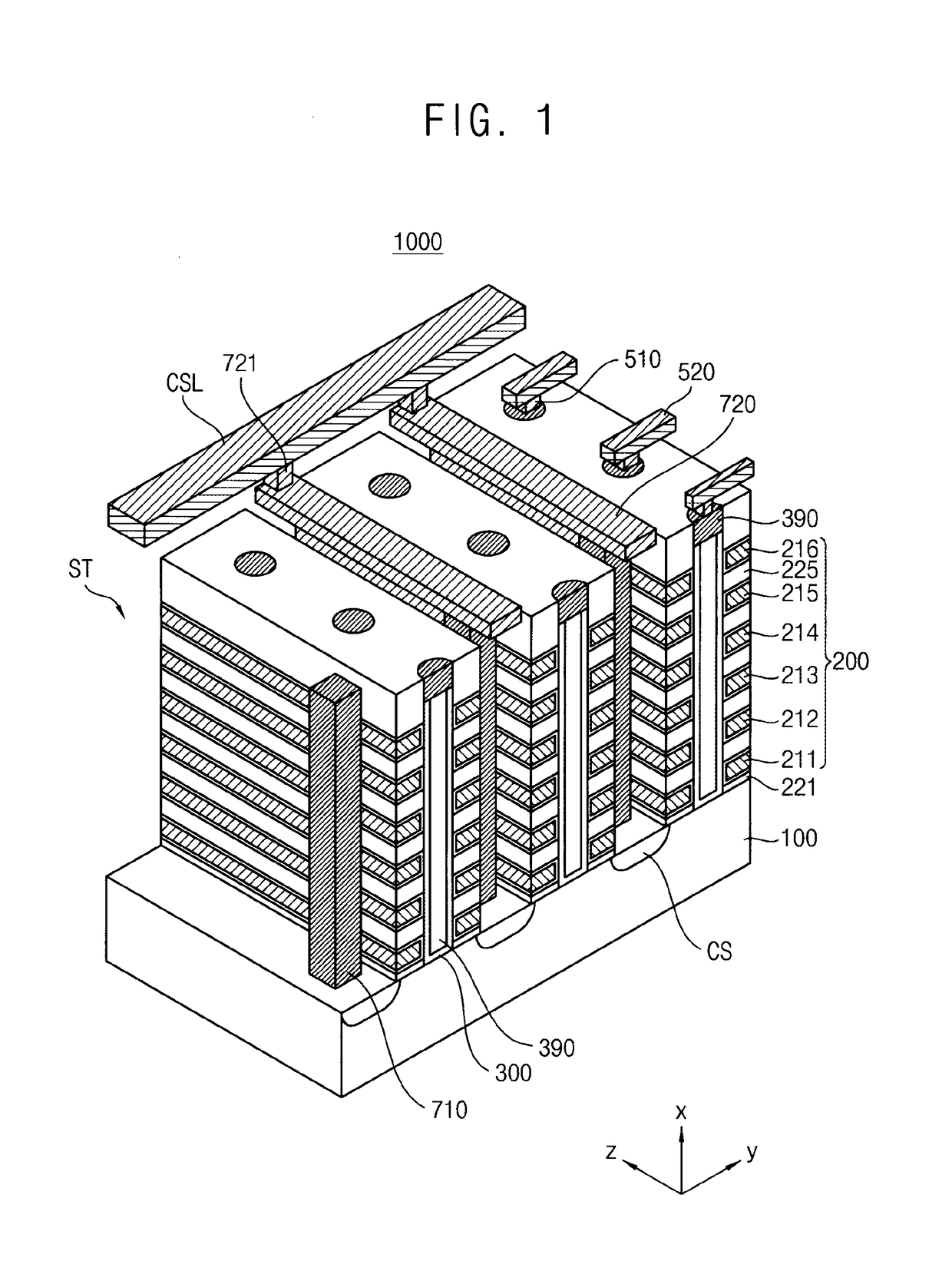
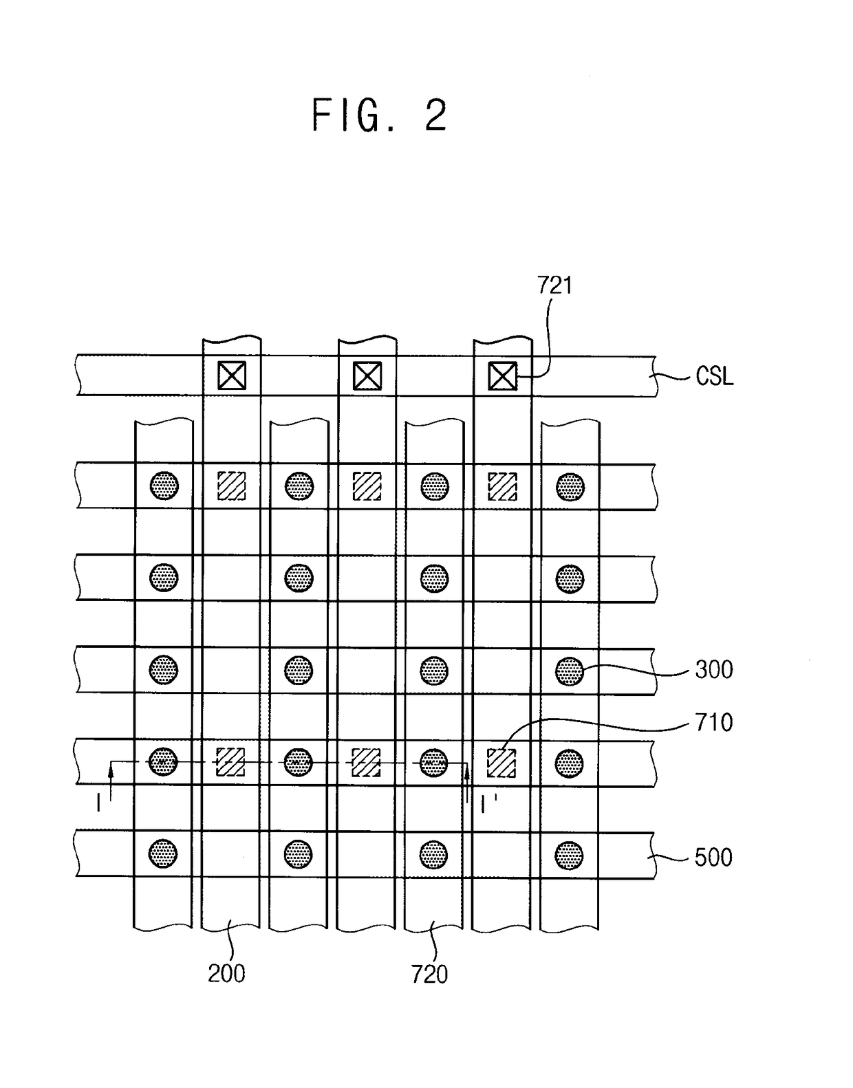
[0030]FIG. 1 is a perspective view illustrating a vertical non-volatile memory device in accordance with some example embodiments of inventive concepts, and FIG. 2 is a plan view illustrating the vertical non-volatile memory device shown in FIG. 1. FIG. 3 is a cross sectional view illustrating the vertical non-volatile memory device shown in FIG. 1 cut along a line I-I′ of FIG. 2. FIG. 4 is an enlarged view of a portion A of FIG. 3.

[0031]Referring to FIGS. 1 to 4, the vertical non-volatile memory device 1000 in accordance with some example embodiments of inventive concepts may include a gate stack structure 200 having conductive structures and insulation interlayer structures that are alternately stacked in a first direction x on a substrate 100, an active column 300 penetrating through the gate stac...


PUM


Abstract

Disclosed are vertical memory devices and methods of manufacturing the same. The vertical memory device may include includes a substrate, a gate stack structure and channel structure on the substrate, and a charge trap structure between the gate stack structure and the channel structure. The gate stack structure includes conductive structures and insulation interlayer structures that are alternately stacked on each other in a vertical direction on the substrate such that cell regions and inter-cell regions are alternately arranged in the vertical direction. The channel structure penetrates through the gate stack structure in the vertical direction. The charge trap structure and the conductive structures define memory cells at the cell regions. The charge structure is configured to selectively store charges. The charge trap structure includes an anti-coupling structure in the inter-cell region for reducing a coupling between neighboring memory cells adjacent to each other in the vertical direction.

Description

CROSS-REFERENCE TO RELATED APPLICATIONS[0001]This application claims priority under 35 U.S.C §119 to Korean Patent Application No. 10-2016-0095738 filed on Jul. 27, 2016 in the Korean Intellectual Property Office, the contents of which are incorporated by reference herein in their entirety.BACKGROUND1. Field[0002]Example embodiments relate to a vertical memory device and a method of manufacturing the same, and more particularly, to a vertical NAND flash memory device and / or a method of manufacturing the same.2. Description of Related Art[0003]A vertical NAND flash memory device in which a plurality of memory cells is vertically stacked on a substrate has been proposed for increasing memory capacity of the NAND memory devices.[0004]As the vertical NAND flash memory device tend to be downsized together with high stack density of the memory cells, the electron diffusion and the cross talk occurs much more frequently between the vertically neighboring stack cells, which affect the relia...

Claims


Application Information

Patent Timeline
Patent Type & Authority Applications(United States)
IPC IPC(8): H01L27/11582H01L27/1157
CPCH01L27/1157H01L27/11582H10B43/30H10B43/10H10B43/20H10B43/35H10B43/27H01L29/7926H10B43/23
Inventor KANAMORI, KOHJIEUN, DONG-SEOG
Owner SAMSUNG ELECTRONICS CO LTD
Why Eureka
Try Eureka