Bandgap reference circuit

a reference circuit and bandgap technology, applied in the direction of electric variable regulation, process and machine control, instruments, etc., can solve the problems of low operating voltage affecting the normal operation of the prior-art bandgap reference circuit, the fabrication process of the schottky diode or the dt mos is not compatible with the standard semiconductor fabrication process,

Inactive Publication Date: 2009-02-26
FARADAY TECH CORP
View PDF6 Cites 27 Cited by
  • Summary
  • Abstract
  • Description
  • Claims
  • Application Information

AI Technical Summary

Benefits of technology

[0031]The present invention provides a bandgap reference circuit including an input circuit having a first FET, a second FET, and a first resistor, wherein a first node is connected to the first FET having a first threshold voltage, the first resistor is connected between a second node and the second FET having a second threshold voltage; a mirroring circuit for controlling two output currents respectively derived from the first and second nodes, and maintaining the two output currents to a specific current ratio; and an operation amplifier connected to the first node, the second node of the input circuit, and the mirroring circuit, for controlling two voltages respectively at the first and second nodes of the input circuit to a specific voltage ratio; wherein the first FET and the second FET are both operating in the subthreshold region, the first threshold voltage is larger than the second threshold voltage, and the two output currents are independent of temperature.
[0032]Furthermore, the present invention provides a bandgap reference circuit, comprising an input circuit having a first FET, a second FET, and a load device, wherein a first node is connected to a first FET having a first threshold voltage, the load device is connected between a second node and the second FET having a second threshold voltage; a mirroring circuit; and, an operation amplifier connected to the mirroring circuit, for controlling the mirroring circuit according a voltage difference between the first node and the second node; wherein the mirroring circuit is capable of generating two output currents respectively derived from the first node and the second node by control of the operation amplifier and maintaining the two output currents to a specific current ratio, and the first FET and the second FET are both operating in the subthreshold region, the first threshold voltage is greater than the second threshold voltage, and the two output currents are independent of temperature.

Problems solved by technology

However, the relatively low operating voltage may affect the normal operation of the prior-art bandgap reference circuit.
However, the fabrication process of the Schottky diode or the DT MOS is not compatible of the standard semiconductor fabrication process.

Method used


Image

  • Bandgap reference circuit
  • Bandgap reference circuit
  • Bandgap reference circuit

Examples


Embodiment Construction

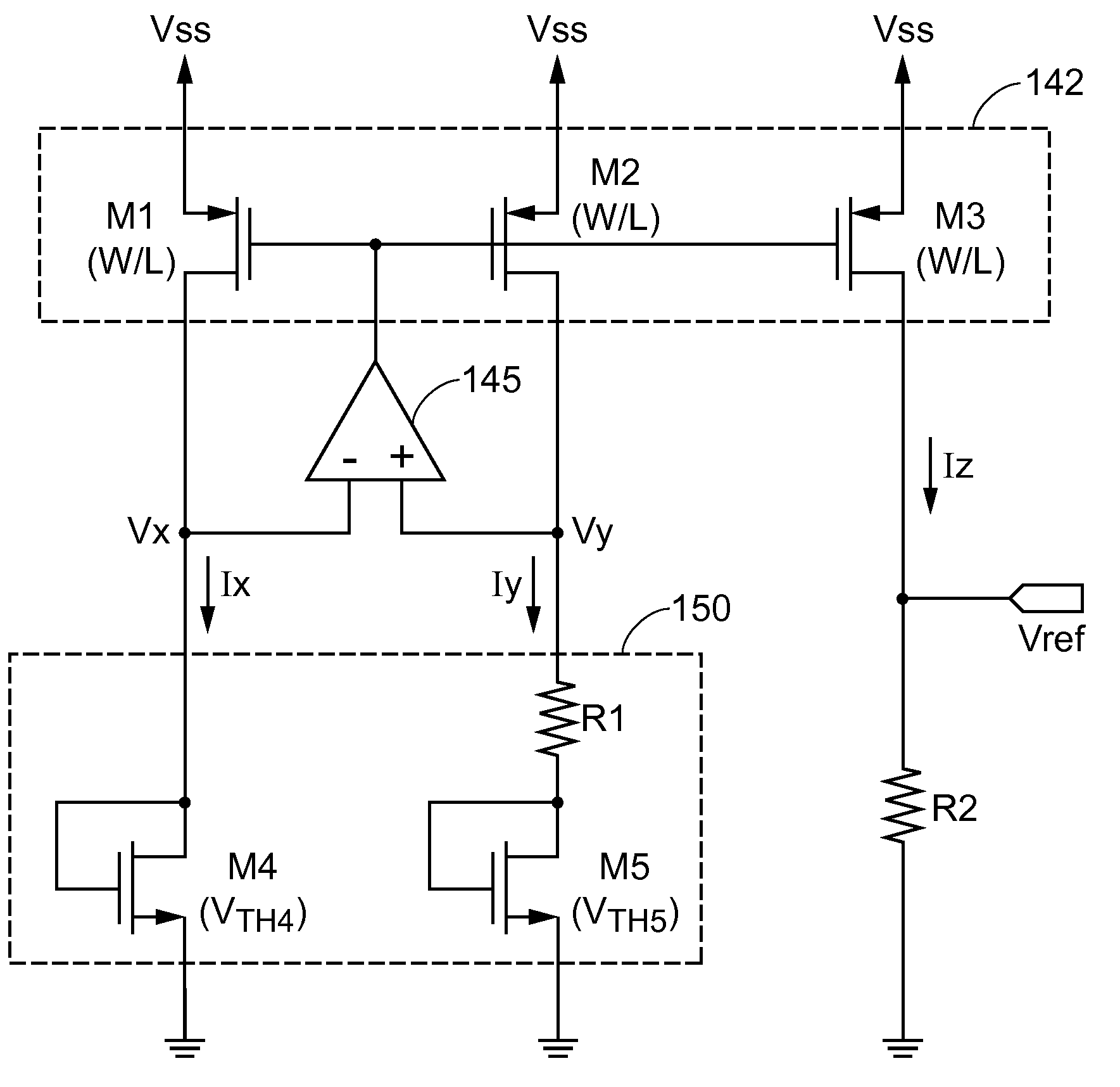
[0045]FIG. 6 is a schematic diagram showing the configuration of a bandgap reference circuit of the present invention. The bandgap reference circuit includes a mirroring circuit 142, an operation amplifier 145 and an input circuit 150. The mirroring circuit 142 comprises three PMOS FETs, M1, M2 and M3. In this example, M1, M2 and M3 have the same aspect ratio (W / L), and the gates of M1, M2 and M3 are connected to one another and the sources of M1, M2 and M3 are connected to a supply voltage (Vss). The drains of M1, M2 and M3 output current Ix, Iy and Iz respectively. Also, an output terminal of the operation amplifier 145 is connected to the gates of M1, M2 and M3 while a positive input terminal of the operation amplifier 145 is connected to the drain of M2 and a negative input terminal of the operation amplifier 145 is connected to the drain of M1. Furthermore, input circuit 150 comprises two NMOS FETs, M4 and M5 and the threshold voltage of M4 is larger than that of M5 (Vth4>Vth5)...


PUM


Abstract

A bandgap reference circuit includes an input circuit having a first FET, a second FET, and a first resistor, wherein a first node is connected to the first FET having a first threshold voltage, the first resistor is connected between a second node and the second FET having a second threshold voltage; a mirroring circuit for controlling two output currents respectively derived from the first and second nodes, and maintaining the two output currents to a specific current ratio; and an operation amplifier connected to the first node, the second node of the input circuit, and the mirroring circuit, for controlling two voltages respectively at the first and second nodes of the input circuit to a specific voltage ratio; wherein the first FET and the second FET are both operating in the subthreshold region, the first threshold voltage is larger than the second threshold voltage, and the two output currents are independent of temperature.

Description

FIELD OF THE INVENTION[0001]The present invention relates to a bandgap reference circuit, and more particularly to a bandgap reference circuit supplied by a low supply voltage.BACKGROUND OF THE INVENTION[0002]As known in the art, a bandgap reference circuit provides a steady reference voltage (Vref) that will not be varied by manufacturing process, temperature or the supply voltage. In the hybrid circuit field, the bandgap reference circuit is designed into many circuits such as voltage regulators, digital to analog converters or low drift amplifier.[0003]Please refer to FIG. 1, which illustrates a conventional bandgap reference circuit implemented by PMOS FETs, PNP BJTs and an operation amplifier. Generally speaking, the bandgap reference circuit includes a mirroring circuit 12, an operation amplifier 15 and an input circuit 20. The mirroring circuit 12 comprises three PMOS FETs, M1, M2 and M3. In this example, M1, M2 and M3 have the same aspect ratio (W / L), and the gates of M1, M2...

Claims


Application Information

Patent Timeline
Patent Type & Authority Applications(United States)
IPC IPC(8): G05F3/16
CPCG05F3/30
Inventor PENG, YAN-HUAUANG, UEI-SHANCHANG, CHIA-WEI
Owner FARADAY TECH CORP
Why Eureka
Try Eureka