Active Matrix Substrate, Display Apparatus, and Television Receiver

Active Publication Date: 2009-03-12
SHARP KK
View PDF52 Cites 24 Cited by
  • Summary
  • Abstract
  • Description
  • Claims
  • Application Information

AI Technical Summary

Benefits of technology

[0048]In this way, the present active matrix substrate makes it possible to reduce inconsistency in capacitance values of capacities (e.g. a storage capacitor, a capacity for controlling an electric poten

Problems solved by technology

This is because it is difficult to perform exposure of the entirety of a large substrate at one time.
Such an exposure process involves problems such as inconsistency in line widths of resist patterns and misalignment, on account of inconsistency in exposure levels between exposure steps.
Inconsistency in line widths of resist patterns (e.g. difference between the widths of storage capac

Method used


Image

  • Active Matrix Substrate, Display Apparatus, and Television Receiver
  • Active Matrix Substrate, Display Apparatus, and Television Receiver
  • Active Matrix Substrate, Display Apparatus, and Television Receiver

Examples


embodiment 1

[0095]The following will describe Embodiment 1 of the present invention with reference to FIG. 1 through FIG. 4 and FIG. 9.

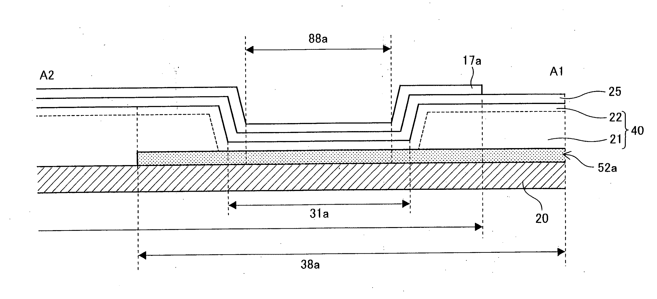
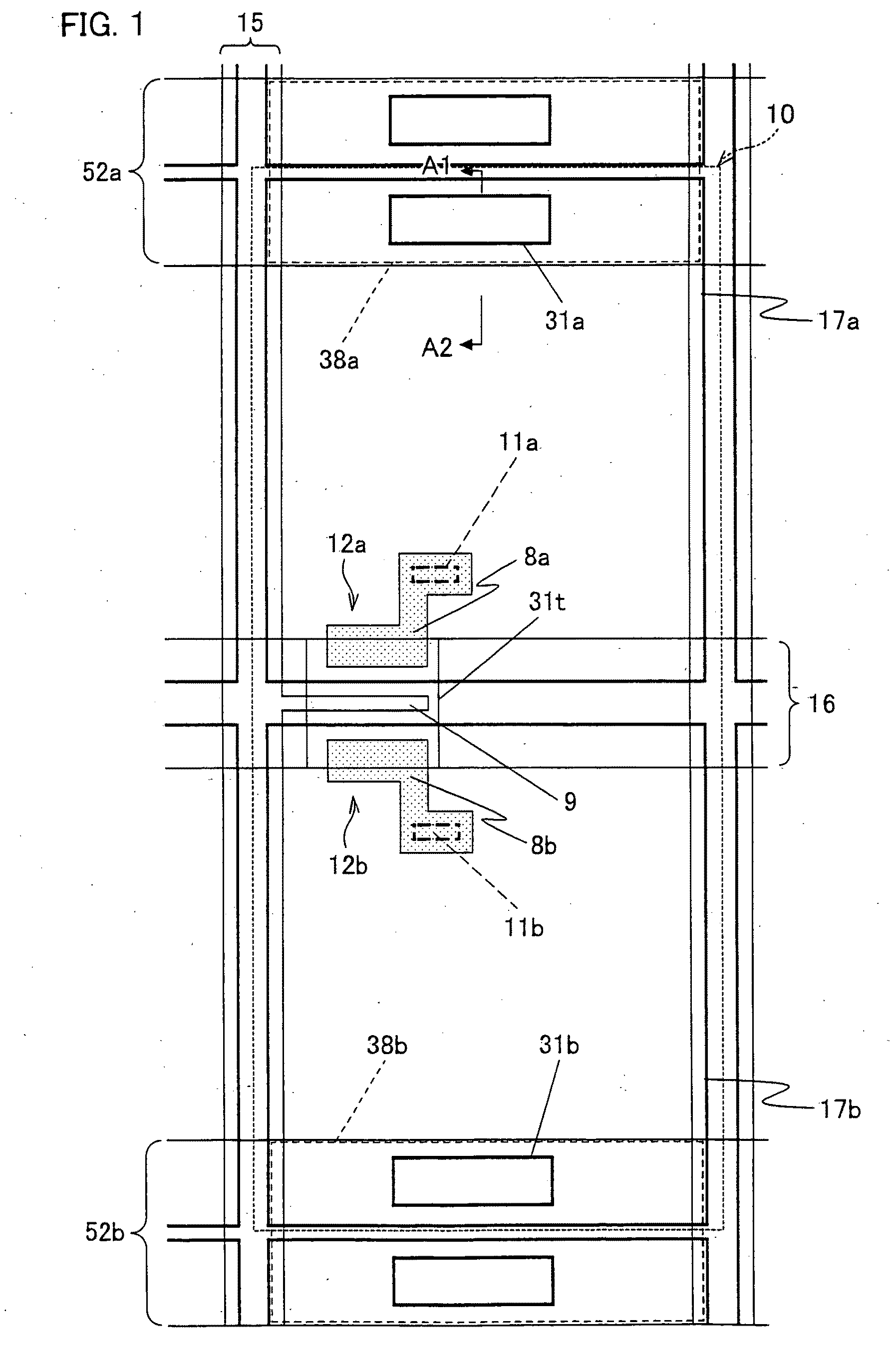
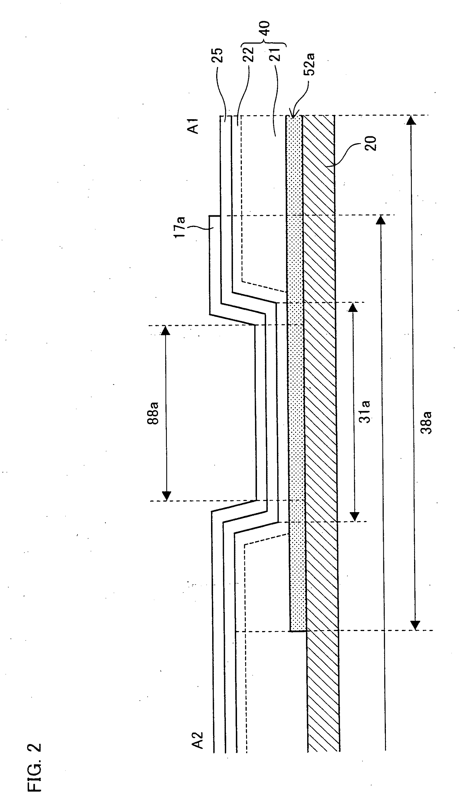
[0096]FIG. 1 is a plan view which outlines an active matrix substrate of the present embodiment. As shown in the figure, the present active matrix substrate is arranged for multi-pixel drive, and each pixel area 10 includes a first TFT (Thin Film Transistor) 12a, a second TFT 12b, a first pixel electrode 17a, a second pixel electrode 17b, a first contact hole 11a, and a second contact hole 11b.

[0097]The present active matrix substrate is further provided with a scanning signal line 16 extending in the horizontal direction in the figure and a data signal line 15 extending in the vertical direction in the figure, which are arranged to be perpendicular to one another. Inside the pixel area 10, the first pixel electrode 17a is provided in the upper half, the second pixel electrode 17b is provided in the lower half, and the scanning signal line 16 traverses the cent...

embodiment 2

[0161]The following will describe Embodiment 2 of the present invention with reference to FIG. 5 through FIG. 8 and FIG. 10.

[0162]FIG. 5 is a plan view which outlines an active matrix substrate of the present embodiment. As shown in the figure, the present active matrix substrate is arranged for multi-pixel drive, and one pixel area 110 includes a first TFT (thin film transistor) 112a, a second TFT 112b, a first pixel electrode 117a, a second pixel electrode 117b, a first drain lead electrode 107a, a first drain lead electrode 107b, a first drain lead line 147a, a first drain lead line 147b, a first contact hole 111a, and a second contact hole 111b.

[0163]The present active matrix substrate is further provided with a scanning signal line 116 extending in the horizontal direction in the figure and a data signal line 115 extending in the vertical direction in the figure, which are arranged to be perpendicular to one another. Inside the pixel area 110, the first pixel electrode 117a is...

embodiment 3

[0190]The present active matrix substrate may be arranged as shown in FIG. 22. FIG. 23 is a cross section at A1-A2 in FIG. 22. As shown in FIG. 22, the present active matrix substrate includes, on each pixel area, a TFT 212, a first pixel electrode 217a and a second pixel electrode 217b (capacity electrodes), a contact hole 211, a control capacity electrode 252 (conductor), and a scanning signal line 216 extending in the horizontal direction in the figure and a data signal line 215 extending in the vertical direction in the figure, which arranged to be perpendicular to each other.

[0191]The control capacity electrode 252 has a rectangular shape which is long along the scanning signal line 216, and overlaps both of the first and second pixel electrodes. As a result of this, a capacity C1 formed by the first pixel electrode 217a and the control capacity electrode 252 is connected in series with a capacity C2 formed by the control capacity electrode 252 and the second pixel electrode 21...


PUM


Abstract

An active matrix substrate of the present invention is arranged so that each pixel area has a transistor and a capacity electrode which is able to function as an electrode of a capacity. The active matrix substrate includes a conductor which is provided in a layer below the capacity electrode and is able to function as the other electrode of the capacity. The gate electrode of each transistor and a gate insulating film covering the conductor have a thin section with reduced thickness, in an on-conductor area overlapping the conductor. At least a part of the thin section overlaps the capacity electrode. In this way, the active matrix substrate which can reduce inconsistency in capacitance values of capacities (e.g. a storage capacitor, a capacity for controlling an electric potential of a pixel electrode, and a capacity which can function as both of them) provided in the substrate.

Description

TECHNICAL FIELD[0001]The present invention relates to an active matrix substrate which is used for a display apparatus such as a liquid crystal display apparatus.BACKGROUND ART[0002]FIG. 30 (see Patent Document 1) is a plan view of a conventional active matrix substrate. As shown in the figure, in each pixel area 750, its pixel electrode 751 is surrounded by a scanning signal line 752 for supplying a scanning signal- and a data signal line 753 for supplying a data signal, in such a manner that these signal lines intersect with one another. At the intersection of the scanning signal line 752 and the data signal line 753, a TFT (Thin Film Transistor) 754 is provided. The gate electrode 755 of the TFT 754 is connected to the scanning signal line 752, so that the TFT 754 is turned on / off in response to the supply of a scanning signal. The source electrode 766 of the TFT 754 is connected to the data signal line 753 and receives a data signal. The drain electrode 777 of the TFT 754 is con...

Claims


Application Information

Patent Timeline
IPC IPC(8): H01L29/04
CPCH01L27/1255G02F1/136213G02F1/1343G02F1/1362G09F9/30H01L29/786G02F1/1368H01L27/1214H01L27/13H01L27/12H01L29/4908
Inventor TSUBATA, TOSHIHIDETAKEUCHI, MASANORI
Owner SHARP KK
Why Eureka
Try Eureka