Plasma display panel and manufacturing method therefor

a technology of display panel and plasma, which is applied in the manufacture of electrode systems, electric discharge tubes/lamps, discharge tubes luminescnet screens, etc., can solve the problems of panel noise, panel bent or otherwise distorted, etc., and achieve the effect of reducing noise, preventing or significantly reducing adverse effects

Inactive Publication Date: 2009-03-12
SAMSUNG SDI CO LTD
View PDF0 Cites 10 Cited by
  • Summary
  • Abstract
  • Description
  • Claims
  • Application Information

AI Technical Summary

Benefits of technology

[0007]Aspects of the present invention provide a plasma display panel capable of reducing noise generated by an inconsistent distance between a front plate and a back plate, and a manufacturing method therefore. Additionally, aspects of the present invention provide a plasma display panel capable of preventing or significantly reducing adverse effects caused by the difference in shrinkage rate of sealant on a long side portion and a short side portion of the panel caused during coupling a back plate to a front plate using the sealant and exhausting it, and a manufacturing method therefore.

Problems solved by technology

In the case of the above-described plasma display panel, the panel may be bent or otherwise distorted due to the difference in shrinkage rate of the barrier ribs and / or sealant, or an unnecessary gap may be created between the front plate and the back plate of the panel during the process of coupling the back plate to the front plate.
The unnecessary gap may lead to an inconsistent distance between the front plate and the back plate of the panel, thereby leading to noise generated in the panel.
In particular, a gap formed in a dummy region of the panel after the coupling process of the panel is one of the main sources of noise generation in the panel.

Method used


Image

  • Plasma display panel and manufacturing method therefor
  • Plasma display panel and manufacturing method therefor
  • Plasma display panel and manufacturing method therefor

Examples


Embodiment Construction

[0024]In the following detailed description, only certain embodiments of the present invention have been shown and described, simply by way of illustration. As those skilled in the art would realize, the described embodiments may be modified in various different ways, all without departing from the spirit or scope of the present invention. Accordingly, the drawings and description are to be regarded as illustrative in nature and not restrictive. In addition, when an element is referred to as being “on” another element, it can be directly on the element or be indirectly on the element with one or more intervening elements interposed therebetween. Hereinafter, like reference numerals refer to like elements.

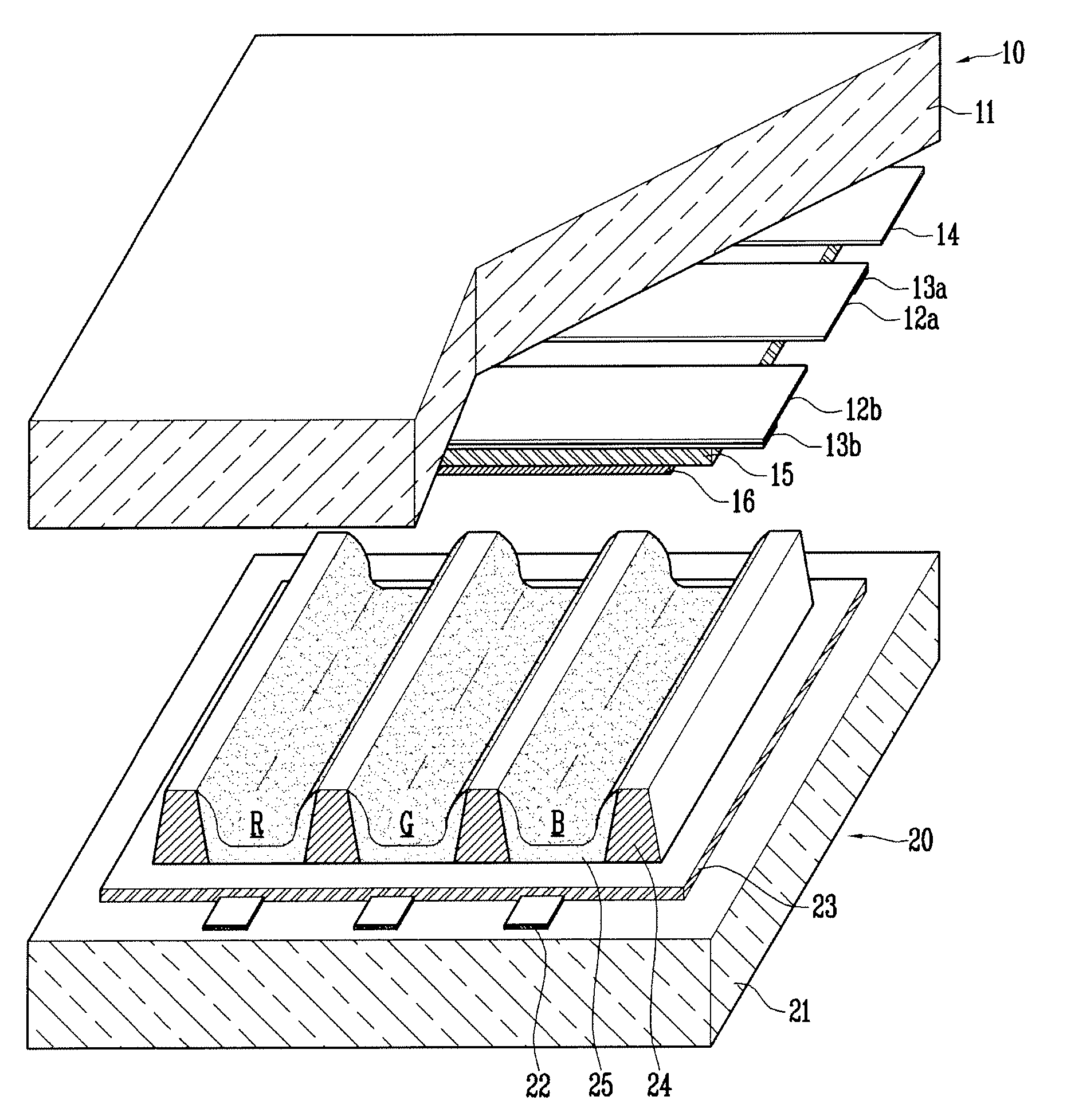
[0025]FIG. 1 is an exploded perspective view showing a PDP according to one embodiment of the present invention.

[0026]Referring to FIG. 1, the PDP includes a front plate 10 and a back plate 20 facing each other. The front plate 10 includes transparent electrodes 12a, 12b, bus electr...


PUM


Abstract

A plasma display panel includes a front plate and a back plate spaced from and facing each other with a barrier rib therebetween, the front plate and the back plate each having a long side and a short side. A first sealant is at the long side between the front plate and the back plate and a second sealant is at the short side between the front plate and the back plate to seal a discharge space divided by the barrier rib between the front plate and the back plate. A first spacer is in the first sealant and a second spacer is in the second sealant, the second spacer having a smaller volume than the first spacer.

Description

CROSS-REFERENCE TO RELATED APPLICATIONS[0001]This application claims priority to and the benefit of Korean Patent Applications No. 10-2007-0092648, filed on Sep. 12, 2007, and No. 10-2008-0028441, filed on Mar. 27, 2008, in the Korean Intellectual Property Office, the entire content of which is incorporated herein by reference.BACKGROUND[0002]1. Field of the Invention[0003]The present invention relates to a plasma display panel and a manufacturing method thereof.[0004]2. Discussion of Related Art[0005]A plasma display panel (PDP) includes a front plate having X-Y electrodes, a dielectric, and an MgO film formed on a transparent substrate; and a back plate having address electrodes, a dielectric, barrier ribs, and phosphors formed on another substrate. The front plate and the back plate are spaced apart from each other by the barrier ribs. Also, the plasma display panel applies a signal to the address electrodes and the Y electrodes through a mounted control circuit to select dischar...

Claims


Application Information

Patent Timeline
Patent Type & Authority Applications(United States)
IPC IPC(8): H01J63/04H01J9/24
CPCH01J9/261H01J11/48H01J11/36H01J11/12
Inventor KWEON, TAE-JOUNG
Owner SAMSUNG SDI CO LTD
Why Eureka
Try Eureka