Method for fabricating pixel structure of active matrix organic light-emitting diode

a technology of organic light-emitting diodes and active matrix, which is applied in the direction of diodes, semiconductor devices, electrical devices, etc., can solve the problems of increasing display size and resolution, affecting the quality of pixel arrays, so as to improve the aperture ratio of pixel arrays, improve frame quality, and improve the effect of frame quality

Active Publication Date: 2009-03-12
IND TECH RES INST
View PDF2 Cites 3993 Cited by
  • Summary
  • Abstract
  • Description
  • Claims
  • Application Information

AI Technical Summary

Benefits of technology

[0009]The present invention is to provide a pixel structure of an active matrix organic light-emitting diode (AMOLED) and the method for fabricating the same, capable of improving the pixel aperture ratio.
[0022]Since the present invention takes two transparent electrodes to form a storage capacitor in the AMOLED pixel structure, the entire capacitor is transparent, which enables to largely increase the aperture ratio of a pixel and allows the capacitor area to be 50%˜95% of a pixel area for improving the frame quality. On the other hand, since the capacitor area in a pixel area can reach 50%˜95%, the frame quality will not be deteriorated even if the size of the pixel is shrunken. Thus, pixel size can be further minimized.
[0023]Note that the gate, the scan line and the data line of the pixel structure are made of low-resistance metal, which contributes to a shorter RC time delay. Hence, the present invention is applicable to fabricate an active matrix panel with high resolution.

Problems solved by technology

However, the luminance efficiency and the lifetime of a passive driving device are largely declined along with the increase of display size and resolution.
Thus, when a color filter is integrated into an OLED panel, the luminance brightness of the pixel array of a bottom emitting AMOLED is obviously not as good as a top emitting AMOLED.

Method used


Image

  • Method for fabricating pixel structure of active matrix organic light-emitting diode
  • Method for fabricating pixel structure of active matrix organic light-emitting diode
  • Method for fabricating pixel structure of active matrix organic light-emitting diode

Examples


Embodiment Construction

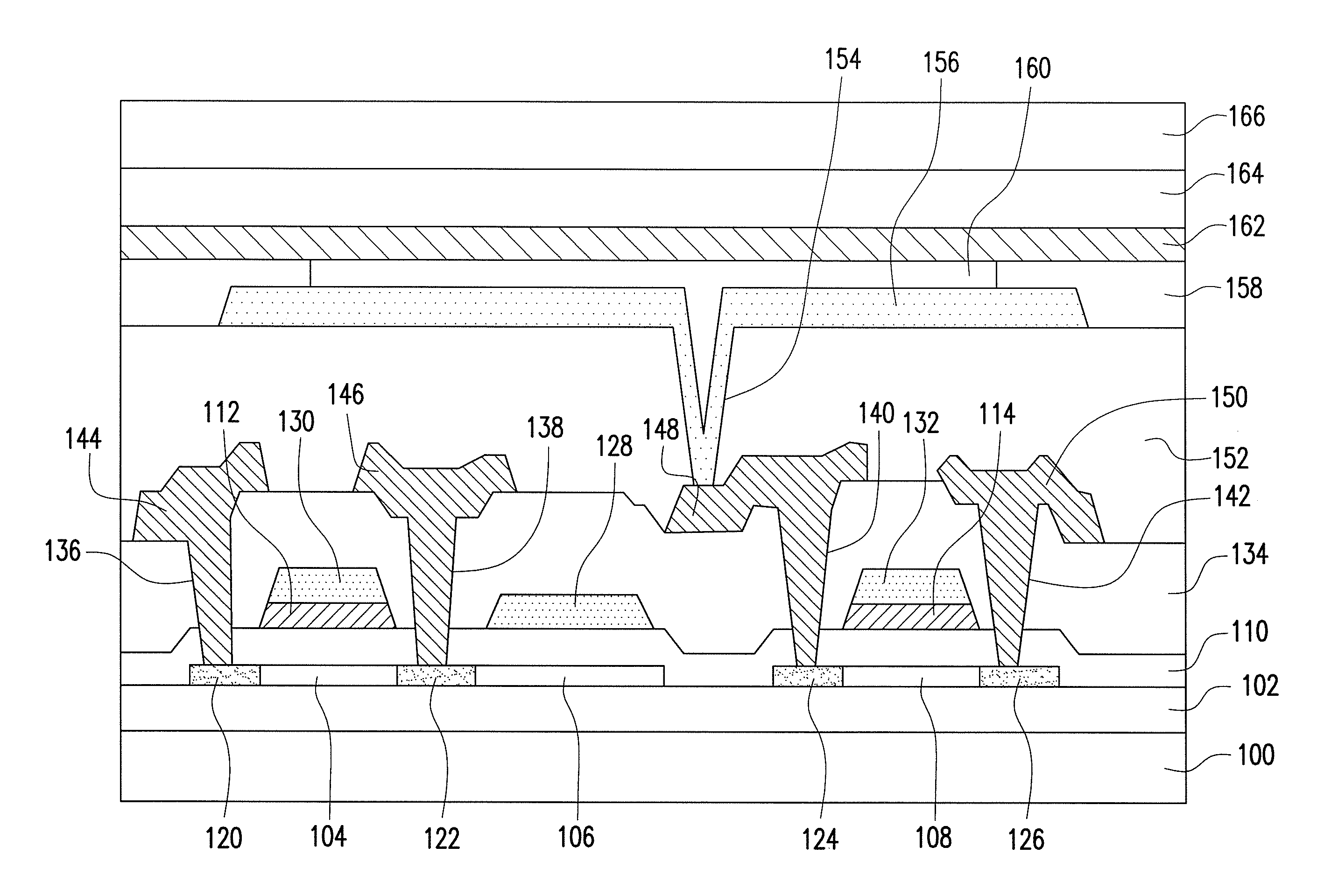
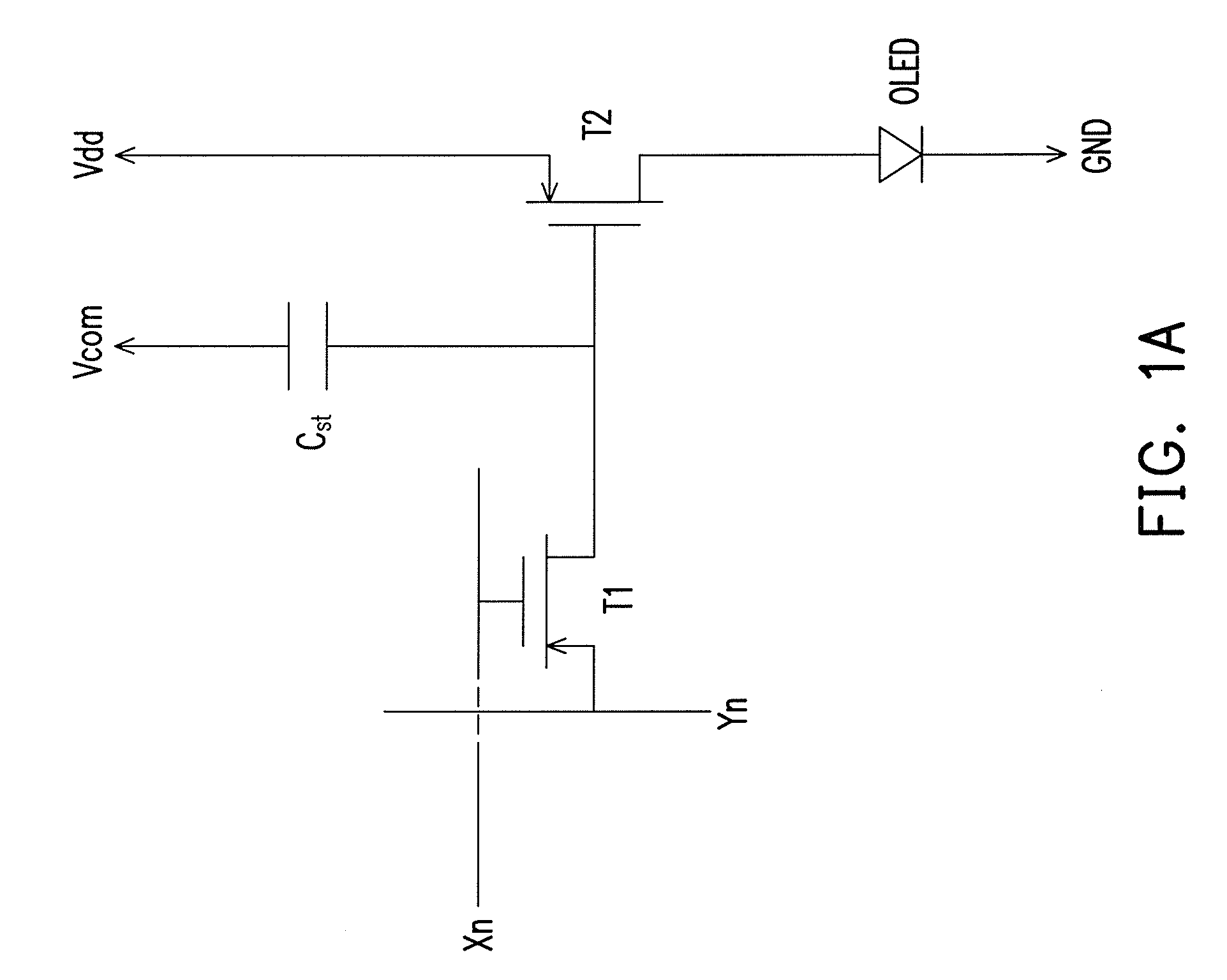
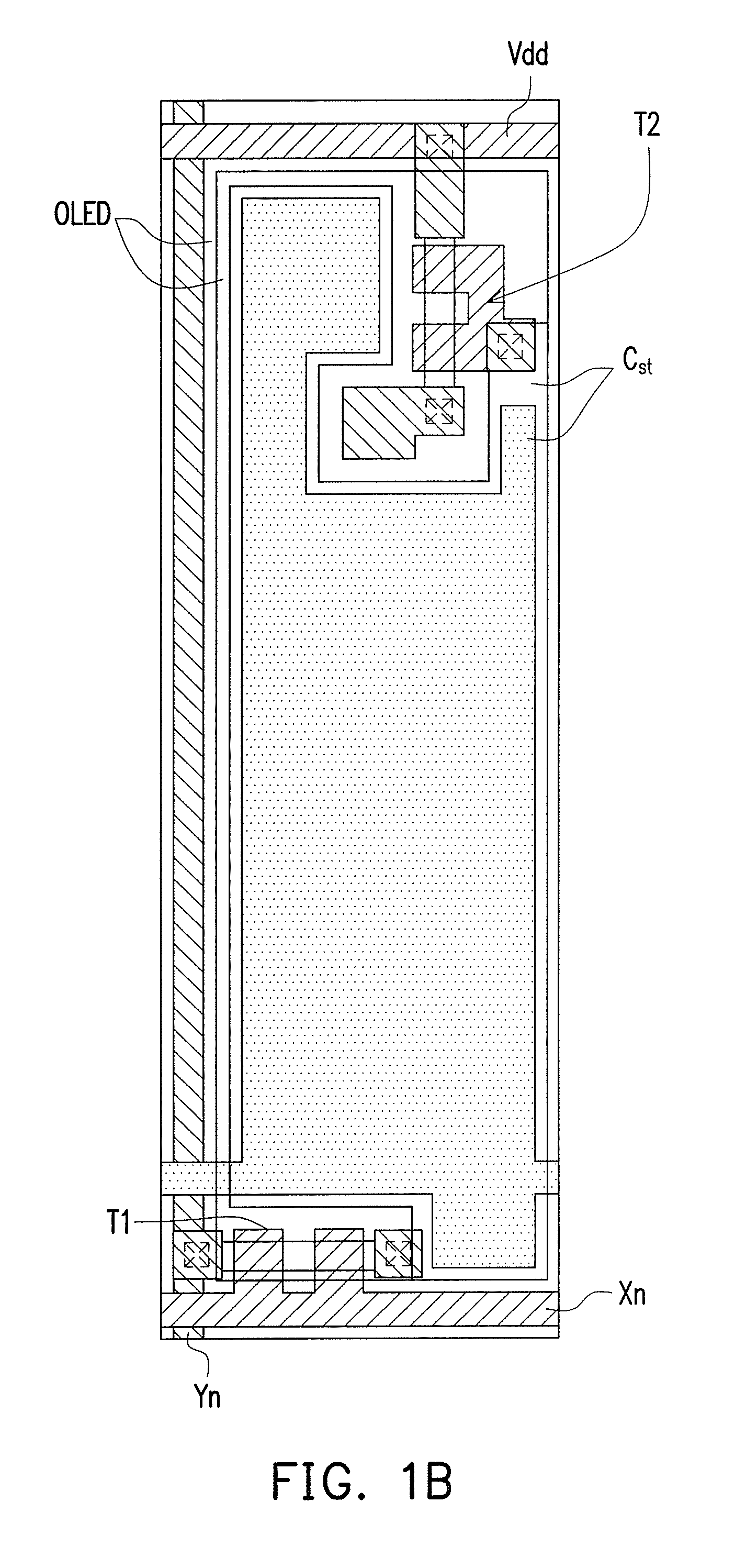
[0029]FIG. 1A is a schematic circuit drawing of an active matrix organic light-emitting diode (AMOLED) pixel structure. Referring to FIG. 1A, an AMOLED is disposed on a transparent substrate and the pixel structure thereof includes an OLED, a data line Yn, a scan line Xn, a switch TFT T1, a driving TFT T2 and a storage capacitor Cst. The gate of the switch TFT T1 is coupled to the scan line Xn, while the source thereof is coupled to the data line Yn and the drain thereof is coupled to the gate of the driving TFT T2 and the storage capacitor Cst. The drain of the driving TFT T2 is coupled to the OLED, while the source thereof is coupled to a power line Vdd. The storage capacitor Cst is formed by two transparent electrodes and a dielectric layer between the two electrodes. The lower electrode of the storage capacitor Cst is electrically connected to the drain of the switch TFT T1 and the gate of the driving TFT T2 and is a transparent semiconductor layer. The material of the transpare...


PUM


Abstract

A method for fabricating an AMOLED pixel includes forming a transparent semiconductor layer on a substrate and forming a first channel layer of the switch TFT, a lower electrode of a storage capacitor and a second channel layer of a driving TFT. A first dielectric layer is formed over the substrate. A first opaque metal gate of the switch TFT, a second opaque metal gate of the driving TFT and a scan line are formed on the first dielectric layer. A first source and a first drain of the switch TFT are formed in the first channel layer and a second source and a second drain of the switch TFT are formed in the second channel layer. A patterned transparent metal layer is formed on the first dielectric layer. A data line is formed over the substrate. An OLED is formed over the substrate.

Description

CROSS-REFERENCE TO RELATED APPLICATION[0001]This application is a divisional of an application Ser. No. 11 / 308,015, filed on Mar. 3, 2006, now pending, which claims the priority benefit of Taiwan application serial no. 94147154, filed on Dec. 29, 2005. The entirety of each of the above-mentioned patent applications is hereby incorporated by reference herein and made a part of this specification.BACKGROUND OF THE INVENTION[0002]1. Field of Invention[0003]The present invention relates to an organic light-emitting diode (OLED) and the method for fabricating the same, and particularly to an active matrix organic light-emitting diode (AMOLED) and the method for fabricating the same.[0004]2. Description of the Related Art[0005]An organic light-emitting diode (OLED) is a semiconductor device capable of converting electrical energy into optical energy. Since OLEDs have advantages of high conversion efficiency, no angle of view (AOV) concern, simpler process, low cost, high response rates, b...

Claims


Application Information

Patent Timeline
Patent Type & Authority Applications(United States)
IPC IPC(8): H01L21/04
CPCH01L27/1225H01L29/7869H01L27/3265H01L27/322H10K59/38H10K59/1216
Inventor LAI, CHIH-MINGYEH, YUNG-HUIHUANG, YI-HSUN
Owner IND TECH RES INST
Why Eureka
Try Eureka