Phase change memory cell in via array with self-aligned, self-converged bottom electrode and method for manufacturing

a memory cell and array technology, applied in the direction of bulk negative resistance effect devices, semiconductor devices, electrical equipment, etc., can solve the problems of reliability and yield issues, difficult to form reliable contact with the underlying access circuitry at the bottom of very small vias, and cells in the array being permanently disconnected from the access circui

Active Publication Date: 2009-03-19
MACRONIX INT CO LTD +1
View PDF99 Cites 99 Cited by
  • Summary
  • Abstract
  • Description
  • Claims
  • Application Information

AI Technical Summary

Benefits of technology

[0023]In technology described herein, the vias, and therefore the memory elements, in the array have respective widths that vary within a distribution that is determined by the lithographic process, or other patterning process, used to form them. The bottom electrodes in the array of bottom electrodes have widths that vary within another distribution that is independent of the patterning process used to form the vias. Thus, the width of a particular via in the array differs from the width of at least one other via in the array of vias by as much as 5% to 10% of the width of the particular via. In contrast, the width of the top surface of the bottom electrode in contact with the memory element within the particular via differs from the width of the top surface of the bottom electrode within the at least one other via by substantially less, such as by 5% to 10% of the overhang dimension, which is much less than said 5% to 10% of the width of the particular via.

Problems solved by technology

Although this technique is suitable for forming very small bottom electrode structures using a plug-in-via process, it has proved to suffer reliability and yield issues.
For example, as described by Ahn et al., it has proven difficult to form reliable contact with the underlying access circuitry at the bottom of very small vias.
This results in some cells in the array being permanently disconnected from the access circuits.
Furthermore, Ahn et al. have related that it is difficult to ensure in the plug-in-via process that the areas of the exposed tops of the plug electrodes are uniform after the planarizing step across a large array of such cells.
Yet another problem arises in the formation of plug-in-via electrodes, because of the difficulty of uniformly filling vias.
In particular, due to the dynamics of thin film deposition within small holes, the plug that results may include a void where the top of the via closes off before it has been completely filled below.
Such holes cause problems in the successful formation of a layer of phase change material over the electrode.
This variation in the critical dimension of a programmable resistive memory cell reduces yield and complicates the technology for programming and reading the data in the cells.
Another problem with manufacturing very small dimension structures is alignment.
These requirements can restrict the flexibility in the design of the memory cells, and cause variation in the performance of the cells.

Method used


Image

  • Phase change memory cell in via array with self-aligned, self-converged bottom electrode and method for manufacturing
  • Phase change memory cell in via array with self-aligned, self-converged bottom electrode and method for manufacturing
  • Phase change memory cell in via array with self-aligned, self-converged bottom electrode and method for manufacturing

Examples


Embodiment Construction

[0034]Embodiments of the present invention are described with reference to FIGS. 1-22.

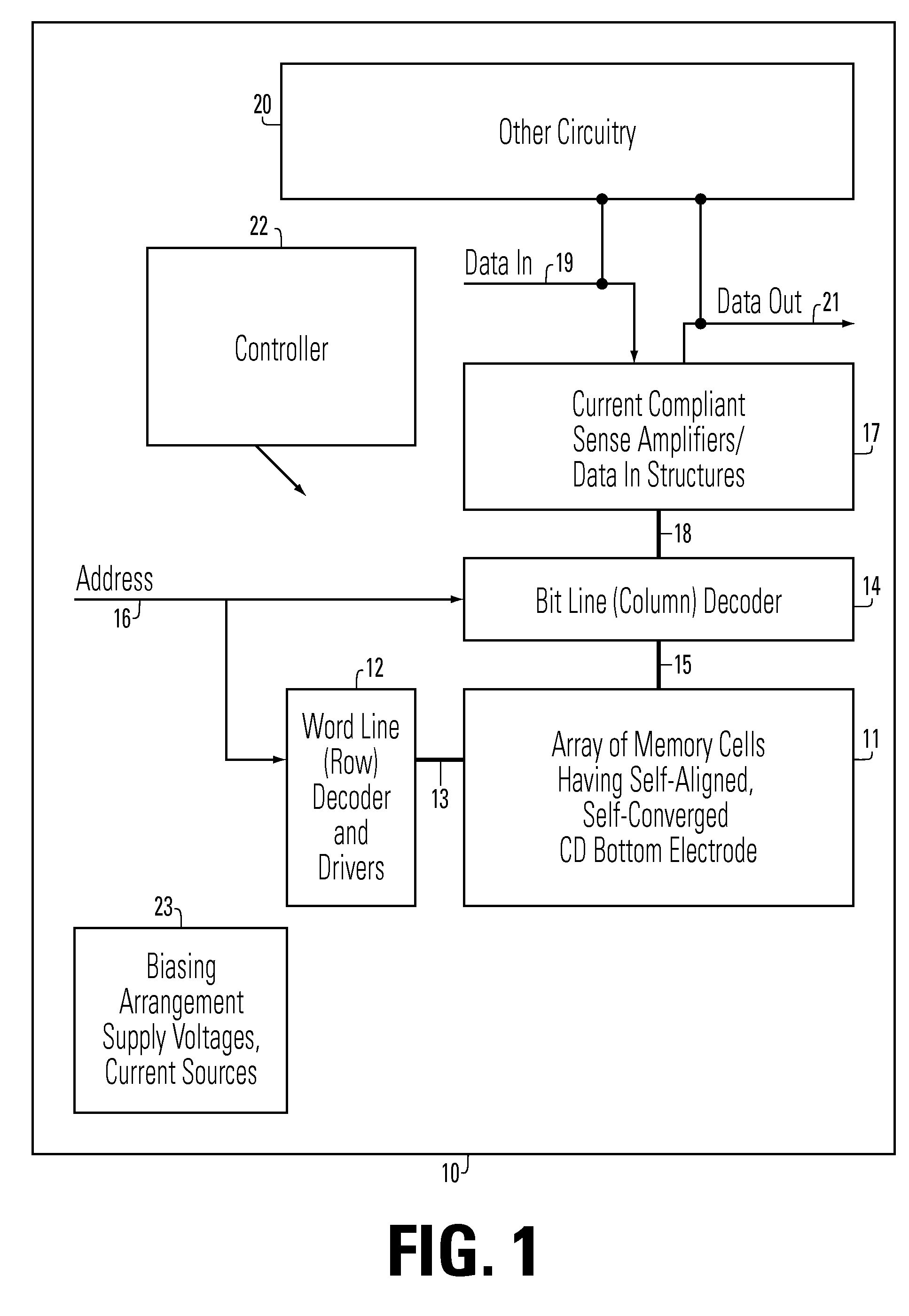
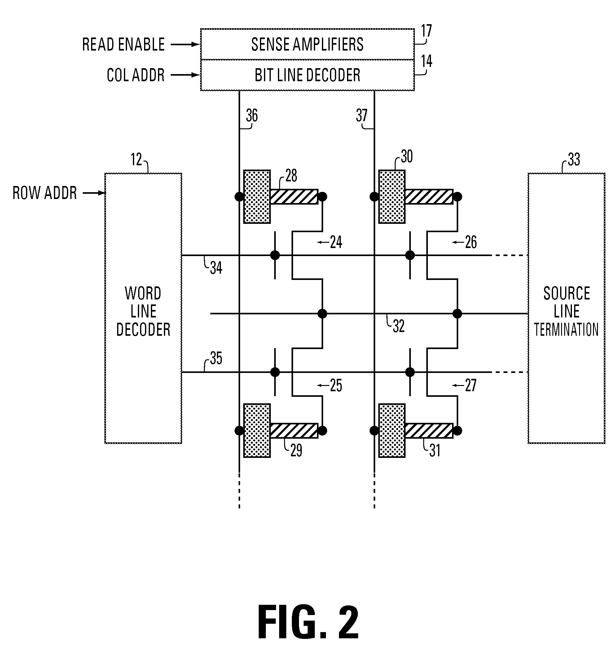
[0035]FIG. 1 is a simplified block diagram of an integrated circuit 10 including a memory array 11 implemented using phase change memory cells as described herein having self-aligned bottom electrodes with self-converged critical dimensions. A word line (or row) decoder 12 is coupled to, and in electrical communication with, a plurality of word lines 13, and arranged along rows in the memory array 11. A bit line (column) decoder 14 is coupled to and in electrical communication with a plurality of bit lines 15 arranged along columns in the memory array 11 for reading data from, and writing data to, the phase change memory cells in the memory array 11. Addresses are supplied on bus 16 to the word line decoder 12 and the bit line decoder 14. Sense amplifiers and data-in structures in block 17, including current sources for the read, set and reset modes, are coupled to the bit line decoder 14 via data ...


PUM


Abstract

An array of "mushroom" style phase change memory cells is manufactured by forming a separation layer over an array of contacts, forming an isolation layer on the separation layer and forming an array of memory element openings in the isolation layer using a lithographic process. Etch masks are formed within the memory element openings by a process that compensates for variation in the size of the memory element openings that results from the lithographic process. The etch masks are used to etch through the separation layer to define an array of electrode openings. Electrode material is deposited within the electrode openings; and memory elements are formed within the memory element openings. The memory elements and bottom electrodes are self-aligned.

Description

BACKGROUND[0001]1. Field of the Invention[0002]The present disclosure relates to high density memory devices based on programmable resistive materials, including phase change materials like chalcogenides, and to methods for manufacturing such devices.[0003]2. Description of Related Art[0004]Programmable resistive materials, including phase change based materials, have been used in nonvolatile random access memory cells. Phase change materials, such as chalcogenides, can be caused to change phase between an amorphous state and a crystalline state by application of electrical current at levels suitable for implementation in integrated circuits. The generally amorphous state is characterized by higher resistivity than the generally crystalline state, which can be readily sensed to indicate data.[0005]Phase change materials are capable of being switched between a first structural state in which the material is in a generally amorphous solid phase, and a second structural state in which ...

Claims


Application Information

Patent Timeline
Patent Type & Authority Applications(United States)
IPC IPC(8): H01L45/00
CPCH01L27/2436H01L45/06H01L45/122H01L45/1683H01L45/144H01L45/1625H01L45/1641H01L45/1253
Inventor LUNG, HSIANG LANLAM, CHUNG HON
Owner MACRONIX INT CO LTD
Why Eureka
Try Eureka