Stress relief structures for silicon interposers

a technology of interposer and stress relief, which is applied in the direction of printed circuit stress/warp reduction, printed circuit aspects, basic electric elements, etc., can solve problems such as failure of integrated circuit chip and/or interposer

Active Publication Date: 2009-03-26
GLOBALFOUNDRIES US INC
View PDF7 Cites 36 Cited by
  • Summary
  • Abstract
  • Description
  • Claims
  • Application Information

AI Technical Summary

Problems solved by technology

During operation of the integrated circuit chip, heating of the integrated circuit chip and/or the interposer can occur causing therm...

Method used


Image

  • Stress relief structures for silicon interposers
  • Stress relief structures for silicon interposers
  • Stress relief structures for silicon interposers

Examples


Embodiment Construction

[0015]The stress relief structures in the interposer of the embodiments of the present invention act as reinforcing elements either by imparting compressive forces on the interposers or simply acting to increase the strength of the interposer in the regions of the interposer they are attached to.

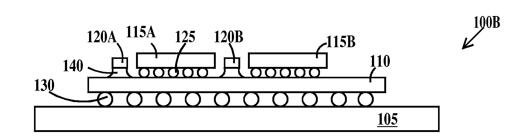
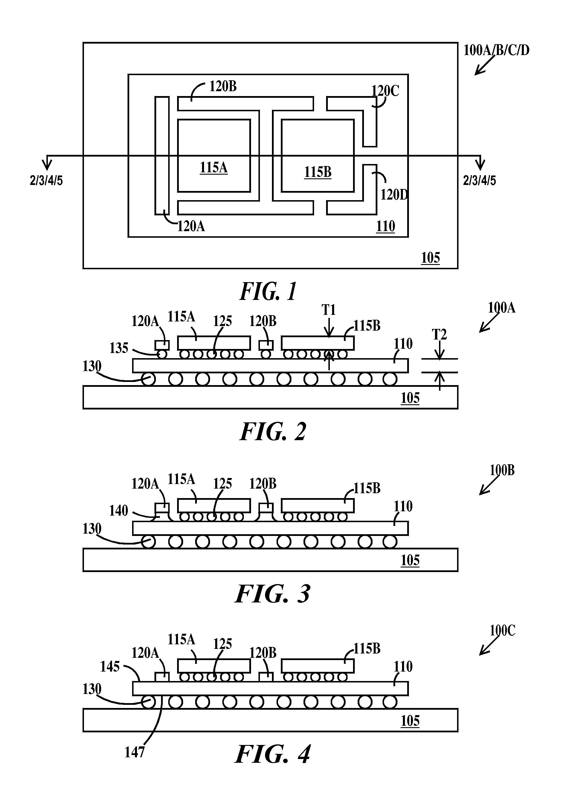
[0016]FIG. 1 a top view of an assembly according to embodiments of the present invention. In FIG. 1, an electronic assembly 100A (or 100B or 100C or 100D) includes a carrier 105, an interposer 110 mounted on and electrically connected to the carrier, integrated circuit chips 115A and 115B mounted on and electrically connected to the interposer, and stress relief structures 120A, 120B, 120C and 120D physically attached to the interposer. In one example, there is no electrical connection between carrier 105, interposer 110 and integrated circuit chips 115A and 115B and stress relief structures 120A, 120B, 120C and 120D. In one example, when stress relief structures 120A, 120B, 120C and 120D co...


PUM


Abstract

An electronic device and method of making the device. The device includes: a carrier; a silicon interposer connected to a top surface of the carrier, the interposer having wires extending from a top surface of the interposer, through the interposer, to a bottom surface of the interposer, the wires at the bottom surface of the interposer electrically connected to wires in a top surface of the carrier; an integrated circuit chip connected to the top surface of the interposer, wires at a surface of the integrated circuit chip electrically connected to the wires in the top surface of the interposer; and a stress relief structure attached to the interposer, the stress relief structure either (i) not electrically connected to the wires of the interposer or integrated circuit chip or (ii) electrically connected to ground by wires of the interposer or wires of the integrated circuit chip.

Description

FIELD OF THE INVENTION[0001]The present invention relates to the field of integrated circuit devices; more specifically, it relates to stress relieved interposer structures and methods of fabricating stress relieved interposer structures.BACKGROUND OF THE INVENTION[0002]An interposer is a device with electrical through vias that is inserted between one or more integrated circuit chips and a carrier. The through vias allow the integrated circuit chips to be electrically connected to the carrier. During operation of the integrated circuit chip, heating of the integrated circuit chip and / or the interposer can occur causing thermal expansion of the integrated circuit chip and / or the interposer leading to failures of the integrated circuit chip and / or the interposer. Accordingly, there exists a need in the art to overcome the deficiencies and limitations described hereinabove.SUMMARY OF THE INVENTION[0003]A first aspect of the present invention is a structure, comprising: a carrier; a si...

Claims


Application Information

Patent Timeline
IPC IPC(8): H01L23/488H01L21/58
CPCH01L23/147H01L2224/16235H01L23/49833H01L23/49838H01L23/562H01L24/16H01L2224/16H01L2924/01078H01L2924/04941H01L2924/14H01L2924/15311H05K1/0271H05K1/0306H05K1/141H05K2201/09781H05K2201/2009H01L23/49822
Inventor WEBB, BUCKNELL CHAPMAN
Owner GLOBALFOUNDRIES US INC
Why Eureka
Try Eureka