Integrated memory management and memory management method

a memory management and memory management technology, applied in the field of integrated memory management and memory management methods, can solve the problems of difficult to realize the control of bad blocks and difficult to effect optimization between different hierarchy operations

Active Publication Date: 2009-03-26
KIOXIA CORP
View PDF16 Cites 211 Cited by
  • Summary
  • Abstract
  • Description
  • Claims
  • Application Information

AI Technical Summary

Benefits of technology

[0015]An integrated memory management device according to the first example of the invention comprises an acquiring unit acquiring a read destination logical address from a first processor of one or more processors; an address conversion unit converting the read destination logical address acquired by the acquiring unit into a read destination physical address of a non-volatile main memory; an access unit reading, from the non-volatile main memory, dat

Problems solved by technology

For this reason, it is difficult to effect optimization between different hierarchy operations.
In this case, it is difficult to realize

Method used


Image

  • Integrated memory management and memory management method
  • Integrated memory management and memory management method
  • Integrated memory management and memory management method

Examples


first embodiment

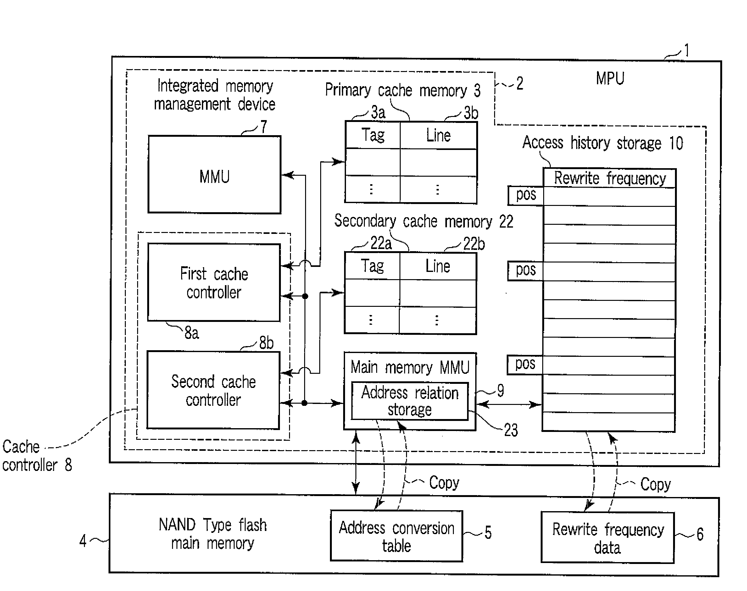
[0044]An integrated memory management device (flat memory management device) of this embodiment is included in a MPU. The integrated memory management device makes memory management with respect to a cache memory and a main memory. The integrated memory management device reduces the number of memory hierarchies related to memory access, and easily realizes optimization of memory access.

[0045]The first embodiment relates to the integrated memory management device, which are integrated with a MMU of MPU, a cache controller of MPU and a main memory MMU.

[0046]FIG. 1 is a block diagram showing an example of the integrated memory management device according to the first embodiment. This embodiment describes the case where a NAND type flash memory is used as the main memory. However, in this case, other memory may be used. According to this embodiment, the term, “access” includes at least one of read and write of data (or program).

[0047]A MPU 1 includes an integrated memory management devi...

second embodiment

[0115]The second embodiment relates to a modification example of the foregoing first embodiment.

[0116]FIG. 6 is a bloc diagram showing an example of an integrated memory management device according to the second embodiment.

[0117]A MPU 11 includes an integrated memory management device 12 according to the second embodiment. An integrated MMU 13 realizes a function of integrating the MMU7 and the main memory MMU 9 of the first embodiment.

[0118]According to the second embodiment, each tag of the primary and secondary cache memories 3 and 22 is used for managing these cache memories 3 and 22 using a process ID and a logical address.

[0119]According to this embodiment, the integrated MMU 13 of a processor, that is, MPU 11 executes a memory mapping management of primary and secondary cache memories 3, 22 and the NAND type flash main memory 4. In this way, various memories are integrally managed.

[0120]FIG. 7 is a view showing an example of a memory hierarchy of the integrated memory managem...

third embodiment

[0126]The third embodiment relates to modification examples of the integrated memory management devices 2 and 12 according to the foregoing first and second embodiments.

[0127]FIG. 8 is a block diagram showing an example of an integrated memory management device 2 according to a modification example of the first embodiment.

[0128]In the foregoing first embodiment, the main memory MMU 9 accesses the NAND type flash main memory 4 based on the physical address. However, the cache controller 8 may execute access to the NAND type flash main memory 4 based on the physical address.

[0129]In this case, the main memory MMU 9 executes control of converting a logical address to a physical location. Then, the cache controller 8 accesses the NAND type flash main memory 4 based on the physical location selected by the main memory MMU 9. According to this embodiment, the cache controller 8 reads and updates the address conversion table 5 and the rewrite frequency data 6 of the NAND type flash main me...


PUM


Abstract

An integrated memory management device according to an example of the invention comprises an acquiring unit acquiring a read destination logical address from a processor, an address conversion unit converting the read destination logical address into a read destination physical address of a non-volatile main memory, an access unit reading, from the non-volatile main memory, data that corresponds to the read destination physical address and has a size that is equal to a block size or an integer multiple of the page size of the non-volatile main memory, and transmission unit transferring the read data to a cache memory of the processor having a cache size that depends on the block size or the integer multiple of the page size of the non-volatile main memory.

Description

CROSS-REFERENCE TO RELATED APPLICATIONS[0001]This is a Continuation-in-Part application of U.S. patent application Ser. No. 12 / 056,501, filed Mar. 27, 2008, the entire contents of which are incorporated herein by reference.[0002]This application is based upon and claims the benefit of priority from prior Japanese Patent Application No. 2007-084272, filed Mar. 28, 2007, the entire contents of which are incorporated herein by reference.BACKGROUND OF THE INVENTION[0003]1. Field of the Invention[0004]The present invention relates to a device and memory management method for managing writing or reading with respect to a cache memory and a main memory.[0005]2. Description of the Related Art[0006]Conventionally, a management function of a NAND type flash memory is built into a file system.[0007]A micro processing unit (MPU) is provided with a cache memory. A dynamic random access memory (DRAM) is used as a main memory. When the MPU accesses the NAND type flash memory, an operation is carri...

Claims


Application Information

Patent Timeline
IPC IPC(8): G06F12/02G06F12/00G06F12/10
CPCG06F12/0246G06F2212/7211G06F2212/7201G06F12/0804
Inventor KUNIMATSU, ATSUSHINAKAI, HIROTOSAKAMOTO, HIROYUKIMAEDA, KENICHI
Owner KIOXIA CORP
Why Eureka
Try Eureka